|
|
PDF NCP1395B Data sheet ( Hoja de datos )
| Número de pieza | NCP1395B | |
| Descripción | High Performance Resonant Mode Controller | |
| Fabricantes | ON Semiconductor | |
| Logotipo | ||
Hay una vista previa y un enlace de descarga de NCP1395B (archivo pdf) en la parte inferior de esta página. Total 27 Páginas | ||
|
No Preview Available !
www.DataSheet4U.com
NCP1395A/B
High Performance Resonant
Mode Controller
The NCP1395A/B offers everything needed to build a reliable and
rugged resonant mode power supply. Its unique architecture includes
a 1.0 MHz Voltage Controller Oscillator whose control mode brings
flexibility when an ORing function is a necessity, e.g. in multiple
feedback paths implementations. Protections featuring various
reaction times, e.g. immediate shutdown or timer−based event,
brown−out, broken optocoupler detection etc., contribute to a safer
converter design, without engendering additional circuitry
complexity. An adjustable deadtime also helps lowering the
shoot−through current contribution as the switching frequency
increases.
Finally, an onboard operational transconductance amplifier allows
for various configurations, including constant output current working
mode or traditional voltage regulation.
Features
• High Frequency Operation from 50 kHz up to 1.0 MHz
• Selectable Minimum Switching Frequency with "3% Accuracy
• Adjustable Deadtime from 150 ns to 1.0 ms
• Startup Sequence via an Adjustable Soft−Start
• Brown−Out Protection for a Simpler PFC Association
• Latched Input for Severe Fault Conditions, e.g. Overtemperature
or OVP
• Timer−Based Input with Auto−Recovery Operation for Delayed
Event Reaction
• Enable Input for Immediate Event Reaction or Simple ON/OFF
Control
• Operational Transconductance Amplifier (OTA) for Multiple
Feedback Loops
• VCC Operation up to 20 V
• Low Startup Current of 300 mA Max
• Common Collector Optocoupler Connection
• Internal Temperature Shutdown
• B Version Features 10 V VCC Startup Threshold for Auxiliary
Supply Usage
• Easy No−Load Operation and Low Standby Power Due to
Programmable Skip−Cycle
• These are Pb−Free Devices*
Typical Applications
• LCD/Plasma TV Converters
• High Power Ac−DC Adapters for Notebooks
• Industrial and Medical Power Sources
• Offline Battery Chargers
http://onsemi.com
MARKING
DIAGRAMS
16
1
PDIP−16
P SUFFIX
CASE 648
16
NCP1395xP
AWLYYWWG
1
16
1
SO−16
D SUFFIX
CASE 751B
1395xDR2G
AWLYWW
x
A
WL
YY, Y
WW
G
= A or B
= Assembly Location
= Wafer Lot
= Year
= Work Week
= Pb−Free Package
PIN CONNECTIONS
Fmin 1
Fmax 2
DT 3
Css 4
FB 5
Ctimer 6
BO 7
AGnd 8
16 NINV
15 Out
14 Slow Fault
13 Fast Fault
12 Vcc
11 B
10 A
9 PGnd
(Top View)
ORDERING INFORMATION
See detailed ordering and shipping information in the package
dimensions section on page 25 of this data sheet.
*For additional information on our Pb−Free strategy
and soldering details, please download the ON
Semiconductor Soldering and Mounting Techniques
Reference Manual, SOLDERRM/D.
© Semiconductor Components Industries, LLC, 2006
March, 2006 − Rev. 1
1
Publication Order Number:
NCP1395/D
1 page 
NCP1395A/B
MAXIMUM RATINGS
Rating
Symbol
Value
Unit
Power Supply Voltage, Pin 12
Transient Current Injected into VCC when Internal Zener is Activated –
Pulse Width < 10 ms
VCC
−
20 V
10 mA
Power Supply Voltage, All Pins (Except Pins 10 and 11)
−
−0.3 to 10
V
Thermal Resistance, Junction−to−Air, PDIP Version
Thermal Resistance, Junction−to−Air, SOIC Version
Storage Temperature Range
RqJA
RqJA
−
TBD
TBD
−60 to +150
°C/W
°C/W
°C
ESD Capability, HBM Model (All Pins Except VCC and HV)
− 2 kV
ESD Capability, Machine Model
− 200 V
Stresses exceeding Maximum Ratings may damage the device. Maximum Ratings are stress ratings only. Functional operation above the
Recommended Operating Conditions is not implied. Extended exposure to stresses above the Recommended Operating Conditions may affect
device reliability.
1. This device series contains ESD protection and exceeds the following tests:
Human Body Model 2000 V per Mil−Std−883, Method 3015
Machine Model Method 200 V.
2. This device contains latch−up protection and exceeds 100 mA per JEDEC Standard JESD78.
http://onsemi.com
5
5 Page 
NCP1395A/B
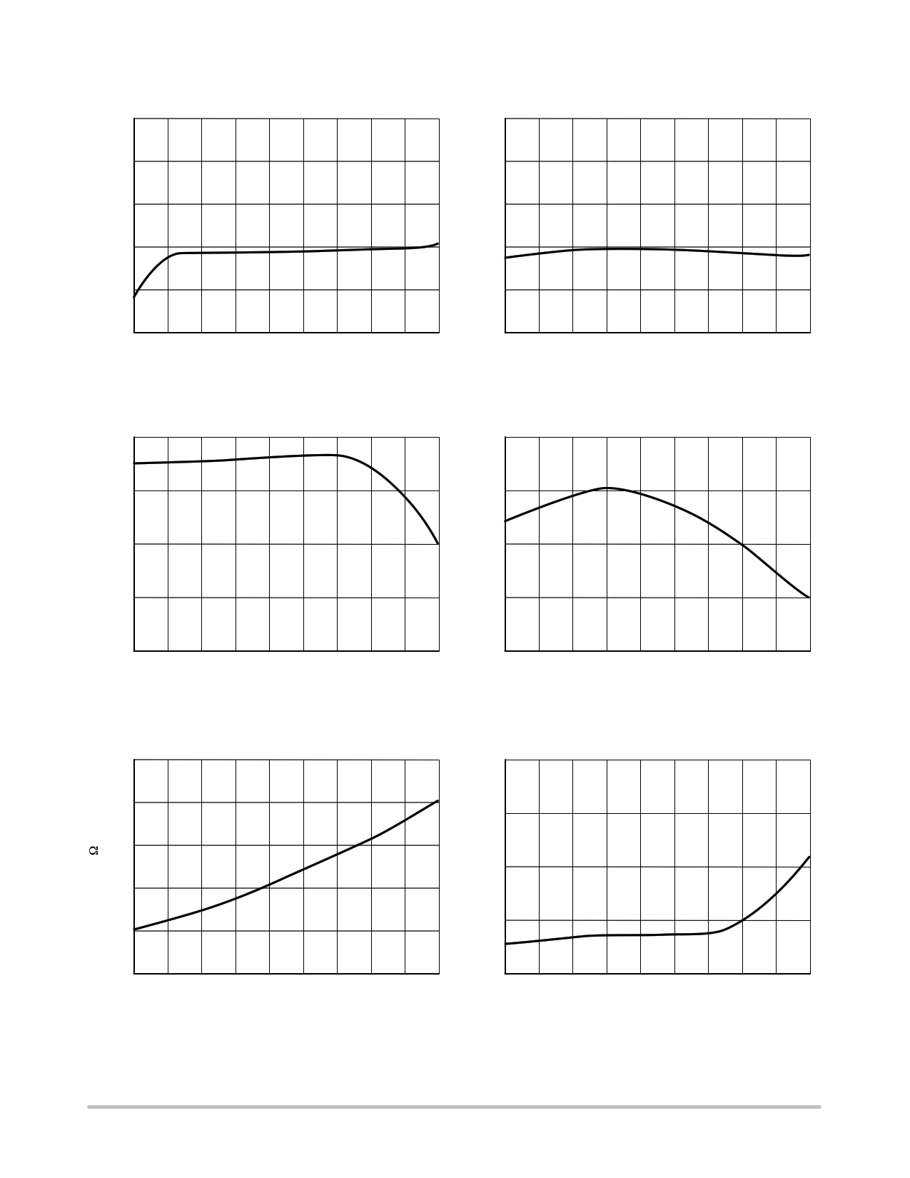
TYPICAL CHARACTERISTICS − B VERSION
11 10
10.8 9.8
10.6 9.6
10.4 9.4
10.2 9.2
10
−40 −20
0 20 40 60 80 100 120 140
TEMPERATURE (°C)
Figure 18. VCCon B
9.0
−40 −20 0
20 40 60 80 100 120 140
TEMPERATURE (°C)
Figure 19. VCCmin
50 1.1
49.5 1.0
49 0.9
48.5 0.8
48
−40 −20 0
20 40 60 80 100 120 140
TEMPERATURE (°C)
Figure 20. Fsw min
0.7
−40 −20 0
20 40 60 80 100 120 140
TEMPERATURE (°C)
Figure 21. Fsw max
23 2.70
22
2.65
21
2.60
20
2.55
19
18
−40 −20 0
20 40 60 80 100 120 140
TEMPERATURE (°C)
Figure 23. Pulldown Resistor (RFB)
2.50
−40 −20 0
20 40 60 80 100 120 140
TEMPERATURE (°C)
Figure 22. Reference (Vref_FB)
http://onsemi.com
11
11 Page | ||
| Páginas | Total 27 Páginas | |
| PDF Descargar | [ Datasheet NCP1395B.PDF ] | |
Hoja de datos destacado
| Número de pieza | Descripción | Fabricantes |
| NCP1395A | High Performance Resonant Mode Controller | ON Semiconductor |
| NCP1395B | High Performance Resonant Mode Controller | ON Semiconductor |
| Número de pieza | Descripción | Fabricantes |
| SLA6805M | High Voltage 3 phase Motor Driver IC. |
Sanken |
| SDC1742 | 12- and 14-Bit Hybrid Synchro / Resolver-to-Digital Converters. |
Analog Devices |
|
DataSheet.es es una pagina web que funciona como un repositorio de manuales o hoja de datos de muchos de los productos más populares, |
| DataSheet.es | 2020 | Privacy Policy | Contacto | Buscar |
