|
|
|
PDF NCP1603 Data sheet ( Hoja de datos )
| Número de pieza | NCP1603 | |
| Descripción | PFC/PWM Combo Controller | |
| Fabricantes | ON Semiconductor | |
| Logotipo | ||
Hay una vista previa y un enlace de descarga de NCP1603 (archivo pdf) en la parte inferior de esta página. Total 30 Páginas | ||
|
No Preview Available !
NCP1603
PFC/PWM Combo Controller
with Integrated High
Voltage Startup and Standby
Capability
The NCP1603 is a Power Factor Correction (PFC) and Pulse Width
Modulation (PWM) combo controller. It offers extremely low
no−load standby power consumption that is suitable for the
low−power consumer markets. The key features of the device are
listed below.
Features
• This is a Pb−Free Device*
PFC Features
• Near−Unity Power Factor in Discontinuous and Critical Mode
(DCM and CRM)
• Voltage−Mode Operation
• Low Startup and Shutdown Current Consumption
• Programmable Switching Frequency for DCM
• Synchronization Capability
• Overvoltage Protection (107% of Nominal Output Level)
• Undervoltage Protection or Shutdown
(8% of Nominal Output Level)
• Programmable Overcurrent Protection
• Thermal Shutdown with Hysteresis (95/140°C)
• Undervoltage Lockout with Hysteresis (9.0/10.5 V)
PWM Features
• Integrated Lossless High Voltage Startup Current Source
• 100 kHz PWM Current−Mode Operation with Skipping Cycle
Capability During Standby Condition
• PFC Bias Voltage is Disabled in Standby Condition to Achieve
Extremely Low No−Load Standby Power Consumption
• Fault Protection Implemented by a Timer and Independent of Badly
Coupled Auxiliary Transformer Winding
• Primary Overcurrent Protection and Latched Overvoltage Protection
• Internal 2.5 ms Soft−Start
• "6.4% Frequency Jittering for Improved EMI Performance
• Latched Thermal Shutdown with Hysteresis (140/165°C)
• Undervoltage Lockout with Hysteresis (5.6/7.7/12.6 V)
Applications
• Notebook Adapters
• TV/Monitors
http://onsemi.com
MARKING
DIAGRAM
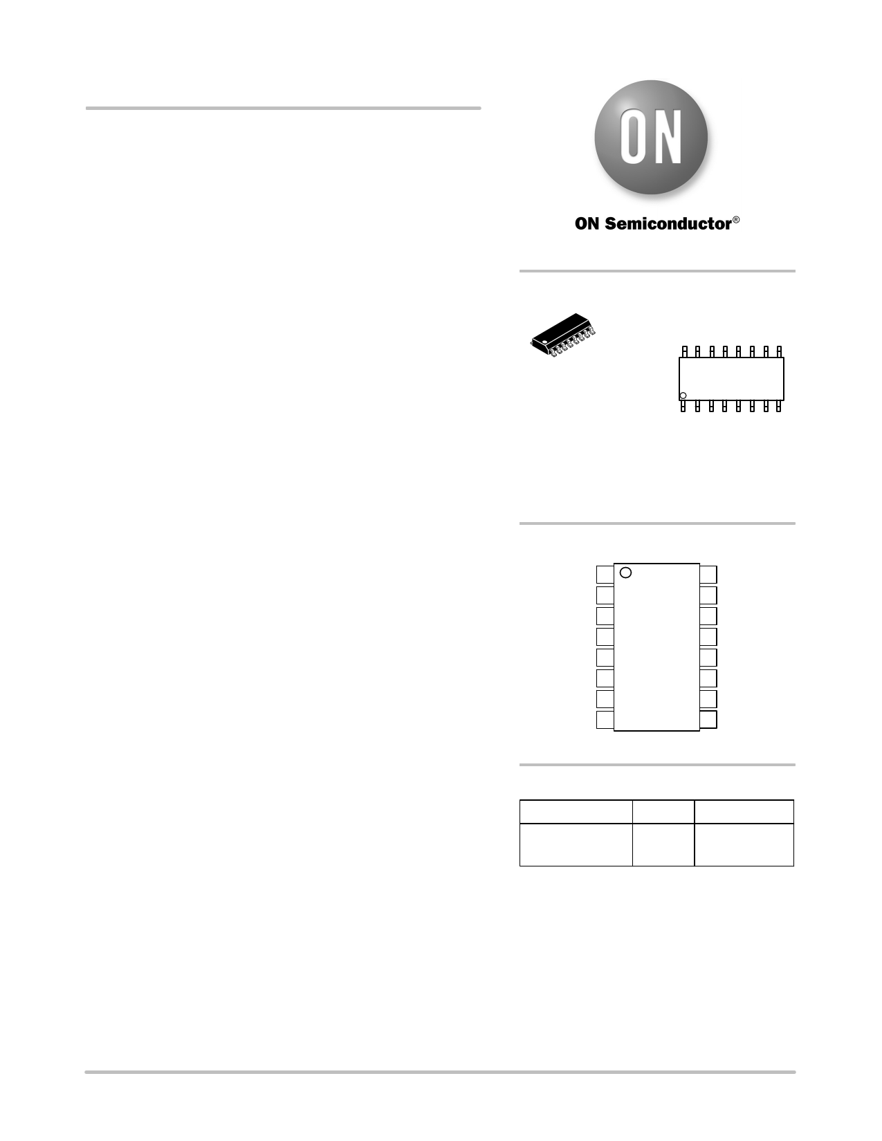
16
1 SO−16
D SUFFIX
CASE 751B
1603D100G
AWLYWW
1
A = Assembly Location
WL = Wafer Lot
Y = Year
WW = Work Week
G = Pb−Free Package
PIN CONNECTIONS
Vaux 1
FB2 2
CS2 3
GND2 4
Osc 5
GND1 6
Out1 7
VCC1 8
(Top View)
16 HV
15 NC
14 VCC2
13 Out2
12 Ramp
11 CS1
10 Vcontrol
9 FB1
ORDERING INFORMATION
Device
Package Shipping†
NCP1603D100R2G SO−16 2500 Tape & Reel
(Pb−Free)
†For information on tape and reel specifications,
including part orientation and tape sizes, please
refer to our Tape and Reel Packaging Specification
Brochure, BRD8011/D.
*For additional information on our Pb−Free strategy and soldering details, please
download the ON Semiconductor Soldering and Mounting Techniques Reference
Manual, SOLDERRM/D.
© Semiconductor Components Industries, LLC, 2009
August, 2009 − Rev. 9
1
Publication Order Number:
NCP1603/D
1 page 
NCP1603
MAXIMUM RATINGS
Rating
Symbol
Value
Unit
Vaux Pin (Pin 1)
Maximum Voltage Range
Maximum Continuous Current
FB2 and CS2 Pin (Pins 2−3)
Maximum Voltage Range
Maximum Current
Vmax
Imax
Vmax
Imax
−0.3 to +18
35
−0.3 to +10
100
V
mA
V
mA
Ramp, CS1, Vcontrol, FB1, and Osc Pins (Pins 5, 9−12)
Maximum Voltage Range
Maximum Current
Out1 Pin (Pin 7)
Maximum Voltage Range
Maximum Current
VCC1 and VCC2 Pins (Pins 8, 14)
Maximum Voltage Range
Maximum Current
Vmax
Imax
Vmax
Imax
Vmax
Imax
−0.3 to +9.0
100
−0.3 to +18
−500 to +750
−0.3 to +18
100
V
mA
V
mA
V
mA
Out2 Pin (Pin 13)
Maximum Voltage Range
Maximum Current
HV Pin (Pin 16)
Maximum Voltage Range
Maximum Current
Vmax
Imax
Vmax
Imax
−0.3 to +17.5
1.0
−0.3 to +500
100
V
A
V
mA
Power Dissipation and Thermal Characteristics
Maximum Power Dissipation (TA = 25°C)
Thermal Resistance, Junction−to−Air
PD
RqJA
770 mW
111 °C/W
Operating Junction Temperature Range
TJ
−40 to +125
°C
Maximum Storage Temperature Range
Tstg
−60 to +150
°C
Stresses exceeding Maximum Ratings may damage the device. Maximum Ratings are stress ratings only. Functional operation above the
Recommended Operating Conditions is not implied. Extended exposure to stresses above the Recommended Operating Conditions may affect
device reliability.
1. This device contains ESD protection and exceeds the following tests:
Pin 1−14: Human Body Model 2000 V per Mil−Std−883, Method 3015.
Machine Model Method 200 V.
Pin 16 is the HV startup of the device and is rated to the maximum rating of the part, or 500 V.
2. This device contains latchup protection and exceeds 100 mA per JEDEC Standard JESD78.
http://onsemi.com
5
5 Page 
NCP1603
250
245
240
235
230
225
220
215
210
205
200
−50
VFB2 = 0.75 V
−25 0
25 50 75 100
TJ, JUNCTION TEMPERATURE (°C)
Figure 15. FB2 Pin Sinking Capability
vs. Temperature
125
160
140
120
100
80
60
40
20
0
−50 −25
0
25 50 75 100 125
TJ, JUNCTION TEMPERATURE (°C)
Figure 16. PWM Section Validation Time for
Recognizing a Fault vs. Temperature
20
18
16
14
12
10
8
6
4
2
0
−50
Vaux = 20 mA Sinking
VCC2 = 13 V
−25 0
25 50 75 100
TJ, JUNCTION TEMPERATURE (°C)
Figure 17. Vaux Pin Internal MOSFET
Resistance vs. Temperature
125
6
5 IHV1 (VCC2 = 0 V)
4
3
2 IHV2 (VCC2 = VCC2(on) − 0.2 V)
1
HV Pin = 30 V
0
−50 −25
0
25 50 75 100 125
TJ, JUNCTION TEMPERATURE (°C)
Figure 18. PWM Section High Voltage Startup
Current Source vs. Temperature
60
50
HV Pin = 700 V
VCC2 = 13 V
40
30
20
10
0
−50 −25
0
25 50 75 100
TJ, JUNCTION TEMPERATURE (°C)
Figure 19. PWM Section HV Pin Leakage
Current vs. Temperature
125
25
24
23
22
21
20
19
18
17
16
15
−50
VCC2 = VCC2(on) − 0.2 V
IHV = 0.5 mA
−25 0
25 50 75 100
TJ, JUNCTION TEMPERATURE (°C)
125
Figure 20. PWM Section HV Pin Minimum
Operating Voltage vs. Temperature
http://onsemi.com
11
11 Page | ||
| Páginas | Total 30 Páginas | |
| PDF Descargar | [ Datasheet NCP1603.PDF ] | |
Hoja de datos destacado
| Número de pieza | Descripción | Fabricantes |
| NCP1600 | High Voltage PFC Controller | ON Semiconductor |
| NCP1601A | Compact Fixed Frequency Discontinuous or Critical Conduction Voltage Mode Power Factor Correction Controller | ON Semiconductor |
| NCP1601B | Compact Fixed Frequency Discontinuous or Critical Conduction Voltage Mode Power Factor Correction Controller | ON Semiconductor |
| NCP1602 | High-Efficiency Power Factor Controller | ON Semiconductor |
| Número de pieza | Descripción | Fabricantes |
| SLA6805M | High Voltage 3 phase Motor Driver IC. |
Sanken |
| SDC1742 | 12- and 14-Bit Hybrid Synchro / Resolver-to-Digital Converters. |
Analog Devices |
|
DataSheet.es es una pagina web que funciona como un repositorio de manuales o hoja de datos de muchos de los productos más populares, |
| DataSheet.es | 2020 | Privacy Policy | Contacto | Buscar |