|
|
PDF NCP5608 Data sheet ( Hoja de datos )
| Número de pieza | NCP5608 | |
| Descripción | Multiple LED Charge Pump Driver | |
| Fabricantes | ON Semiconductor | |
| Logotipo | ||
Hay una vista previa y un enlace de descarga de NCP5608 (archivo pdf) en la parte inferior de esta página. Total 16 Páginas | ||
|
No Preview Available !
www.DataSheet4U.com
NCP5608
Multiple LED Charge Pump
Driver
The NCP5608 is a high efficiency boost converter operating in
current loop, based on a charge pump multi mode, to drive White
LED. The current mode regulation allows a uniform and
programmable brightness of the LEDs. The chip has been optimized
for small ceramic capacitors, capable to supply up to 2.0 W output
power.
Features
• 2.7 to 5.5 V Input Voltage Range
• Up to 500 mA Output Current
• Capable to Drive 8 LED
• Multi Mode Charge Pump Based Converter
• I2C Serial Link Protocol
• Consistent High Efficiency
• Independently Block Programmable Output Currents
• Programmable 3 or 4 Operating Backlight LED at Zero Extra
Losses
• Constant Output Current Regulation
• Built−in Dimming Function
• Tight Automatic LED Current Matching
• Thermal Shutdown Protection
• Low Battery Return Noise
• This is a Pb−Free Device*
Typical Applications
• LED Display Back Light Control
• Keyboard Back Light
• High Power Photo Flash
• Multiple Displays
http://onsemi.com
24 PIN TQFN (4x4)
MT SUFFIX
CASE 511AA
MARKING
DIAGRAM
24
1 NCP
5608
ALYW
G
A = Assembly Location
L = Wafer Lot
Y = Year
W = Work Week
G = Pb−Free Package
PIN CONNECTIONS
24 23 22 21 20 19
AGND 1
18 VOUT
IREFFL 2
17 C1P
IREFBK 3
16 C1N
SDA 4
SCL 5
15 LED8
14 LED7
CCMP 6
13 PGND
7 8 9 10 11 12
*For additional information on our Pb−Free strategy and soldering details, please
download the ON Semiconductor Soldering and Mounting Techniques Reference
Manual, SOLDERRM/D.
ORDERING INFORMATION
Device
Package
Shipping†
NCP5608MTR2G TQFN24 4000 / Tape & Reel
(Pb−Free)
†For information on tape and reel specifications,
including part orientation and tape sizes, please
refer to our Tape and Reel Packaging Specification
Brochure, BRD8011/D.
© Semiconductor Components Industries, LLC, 2006
June, 2006 − Rev. 1
1
Publication Order Number:
NCP5608/D
1 page 
NCP5608
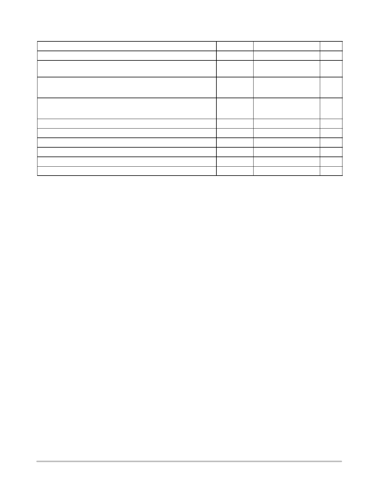
MAXIMUM RATINGS
Rating
Symbol
Value
Unit
Power Supply
Digital Input Voltage
Digital Input Current
Vbat
SDA, SCL
−
7.0
−0.3 v Vin v VBAT + 0.3
1.0
V
V
mA
ESD Capability (Note 4)
Human Body Model (HBM)
Machine Model (MM)
VESD
2.0 kV
200 V
QFN24 Package
Power Dissipation @ TA = +85°C (Note 5)
Thermal Resistance, Junction−to−Air (according to JEDEC/EIA JESD51−12)
Operating Ambient Temperature Range
Operating Junction Temperature Range
Maximum Junction Temperature
Storage Temperature Range
Latchup Current Maximum Rating (per JEDEC standard: JESD78) Class II
PD
RqJA
TA
TJ
TJmax
Tstg
−
250
160
−40 to +85
−40 to +125
+150
−65 to +150
"100
mW
°C/W
°C
°C
°C
°C
mA
Moisture Sensitivity Level (Note 6)
MSL
1−
Stresses exceeding Maximum Ratings may damage the device. Maximum Ratings are stress ratings only. Functional operation above the
Recommended Operating Conditions is not implied. Extended exposure to stresses above the Recommended Operating Conditions may affect
device reliability.
4. This device series contains ESD protection and exceeds the following tests:
Human Body Model (HBM): JESD22−A114.
Machine Model (MM): JESD22−A115.
5. The maximum package power dissipation limit must not be exceeded.
6. Moisture Sensitivity Level (MSL): per IPC/JEDEC standard: J−STD−020A.
http://onsemi.com
5
5 Page 
NCP5608
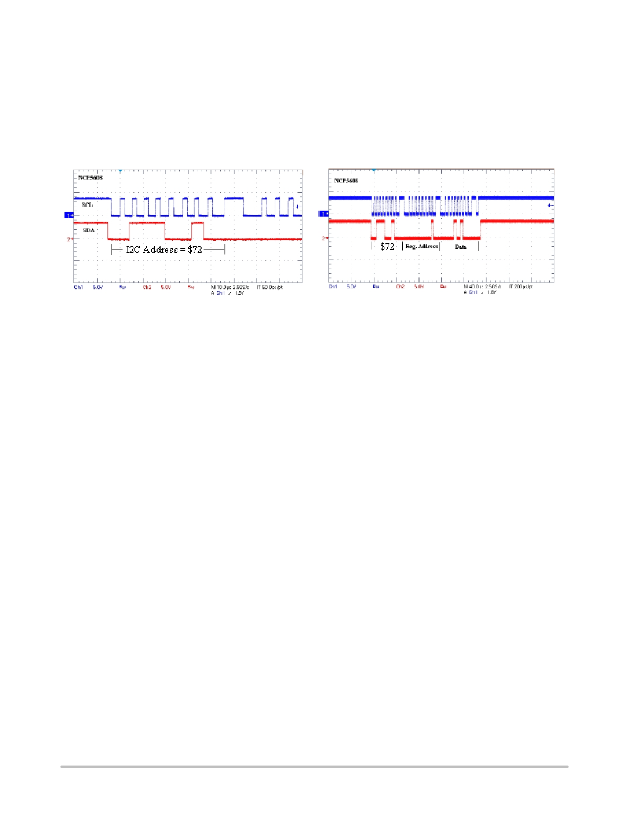
The three bytes, defined to program the chip, must be
sent during the same transaction as depicted in Figure 6 and
Figure 7. Leaving aside the ACK signal, the NCP5608
does not provide any digital feedback. The selected
PWRLED−BK or PWRLED−FL register described above
will be updated according to the content of the third byte
serially sent to the chip. Finally, the selected bank of LED
will be updated on the last I2C clock positive going slope
of the third byte, the DATA being transferred to the
appropriate latchup register as defined by the content of the
second byte.
The DC−DC charge pump is deactivated when both
registers are set to zero as depicted in Table 3.
Figure 6. Typical Transaction I2C Sequence:
I2C Address
Figure 7. Typical Full I2C Data Transfer
http://onsemi.com
11
11 Page | ||
| Páginas | Total 16 Páginas | |
| PDF Descargar | [ Datasheet NCP5608.PDF ] | |
Hoja de datos destacado
| Número de pieza | Descripción | Fabricantes |
| NCP5602 | High Efficiency Ultra Small Thinnest White LED Driver | ON Semiconductor |
| NCP5603 | High Efficiency Charge Pump Converter | ON Semiconductor |
| NCP5604A | High Efficiency White LED Driver | ON Semiconductor |
| NCP5604B | High Efficiency White LED Driver | ON Semiconductor |
| Número de pieza | Descripción | Fabricantes |
| SLA6805M | High Voltage 3 phase Motor Driver IC. |
Sanken |
| SDC1742 | 12- and 14-Bit Hybrid Synchro / Resolver-to-Digital Converters. |
Analog Devices |
|
DataSheet.es es una pagina web que funciona como un repositorio de manuales o hoja de datos de muchos de los productos más populares, |
| DataSheet.es | 2020 | Privacy Policy | Contacto | Buscar |
