|
|
|
PDF NTLJF3118N Data sheet ( Hoja de datos )
| Número de pieza | NTLJF3118N | |
| Descripción | Power MOSFET ( Transistor ) | |
| Fabricantes | ON Semiconductor | |
| Logotipo | ||
Hay una vista previa y un enlace de descarga de NTLJF3118N (archivo pdf) en la parte inferior de esta página. Total 7 Páginas | ||
|
No Preview Available !
www.DataSheet4U.com
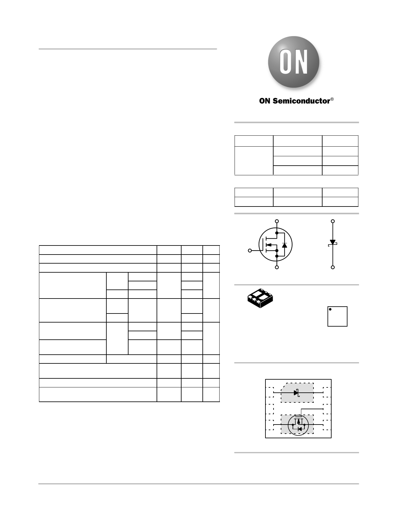
NTLJF3118N
Power MOSFET and
Schottky Diode
20 V, 4.6 A, mCool] N−Channel, with
2.0 A Schottky Barrier Diode, 2x2 mm
WDFN Package
Features
• WDFN 2x2 mm Package Provides Exposed Drain Pad for
Excellent Thermal Conduction
• Footprint Same as SC−88 Package
• 1.8 V VGS Rated RDS(on)
• Low Profile (< 0.8 mm) for Easy Fit in Thin Environments
• Low VF 2 A Schottky Diode
• This is a Pb−Free Device
Applications
• DC−DC Boost/Buck Converter
• Low Voltage Hard Disk DC Power Source
MAXIMUM RATINGS (TJ = 25°C unless otherwise noted)
Parameter
Symbol Value Unit
Drain−to−Source Voltage
VDSS 20 V
Gate−to−Source Voltage
VGS ±12 V
Continuous Drain Current
(Note 1)
Steady TA = 25°C
State TA = 85°C
ID
3.8 A
2.8
t ≤ 5 s TA = 25°C
4.6
Power Dissipation
(Note 1)
Steady
State
t≤5s
TA = 25°C
PD
1.5 W
2.2
Continuous Drain Current
(Note 2)
Power Dissipation
(Note 2)
Steady
State
TA = 25°C
TA = 85°C
TA = 25°C
ID
PD
2.6 A
1.9
0.7
Pulsed Drain Current
tp = 10 ms
Operating Junction and Storage Temperature
Source Current (Body Diode)
Lead Temperature for Soldering Purposes
(1/8″ from case for 10 s)
IDM
TTSJT,G
IS
TL
18
−55 to
150
1.8
260
A
°C
A
°C
Stresses exceeding Maximum Ratings may damage the device. Maximum
Ratings are stress ratings only. Functional operation above the Recommended
Operating Conditions is not implied. Extended exposure to stresses above the
Recommended Operating Conditions may affect device reliability.
1. Surface Mounted on FR4 Board using 2 in sq pad size
(Cu area = 1.127 in sq [2 oz] including traces).
2. Surface Mounted on FR4 Board using the minimum recommended pad size.
© Semiconductor Components Industries, LLC, 2006
October, 2006 − Rev. 0
1
http://onsemi.com
MOSFET
V(BR)DSS
20 V
RDS(on) Max
65 mW @ 4.5 V
75 mW @ 2.5 V
120 mW @ 1.8 V
VR Max
20 V
SCHOTTKY DIODE
VF Typ
0.41 V
ID Max
3.8 A
2.0 A
1.7 A
IF Max
2.0 A
DA
G
S
N−CHANNEL MOSFET
K
SCHOTTKY DIODE
MARKING
DIAGRAM
1
WDFN6
CASE 506AN
16
2 JK M G 5
3 G4
JK = Specific Device Code
M = Date Code
G = Pb−Free Package
(Note: Microdot may be in either location)
PIN CONNECTIONS
A1
K
6K
N/C 2
D3
5G
D
4S
(Top View)
ORDERING INFORMATION
See detailed ordering and shipping information in the package
dimensions section on page 3 of this data sheet.
Publication Order Number:
NTLJF3118N/D
1 page 
NTLJF3118N
TYPICAL N−CHANNEL PERFORMANCE CURVES (TJ = 25°C unless otherwise noted)
600 VDS = 0 V VGS = 0 V
500 Ciss
TJ = 25°C
5
4
QT
20
16
400
300
200 Crss
100
Coss
0
10 5 0 5 10 15 20
VGS
VDS
GATE−TO−SOURCE OR DRAIN−TO−SOURCE VOLTAGE (V)
Figure 7. Capacitance Variation
3 VDS
2 QGS
QGD
VGS 12
8
14
ID = 3.8 A
0 TJ = 25°C 0
01 234
QG, TOTAL GATE CHARGE (nC)
Figure 8. Gate−To−Source and Drain−To−Source
Voltage versus Total Charge
100
VDD = 16 V
ID = 1.0 A
VGS = 4.5 V
10
td(off)
tf
tr
td(on)
2
VGS = 0 V
TJ = 25°C
1.5
1
0.5
1
1 10 100
RG, GATE RESISTANCE (W)
Figure 9. Resistive Switching Time
Variation versus Gate Resistance
0
0.4 0.5 0.6 0.7 0.8 0.9
VSD, SOURCE−TO−DRAIN VOLTAGE (V)
Figure 10. Diode Forward Voltage versus Current
http://onsemi.com
5
5 Page | ||
| Páginas | Total 7 Páginas | |
| PDF Descargar | [ Datasheet NTLJF3118N.PDF ] | |
Hoja de datos destacado
| Número de pieza | Descripción | Fabricantes |
| NTLJF3118N | Power MOSFET ( Transistor ) | ON Semiconductor |
| Número de pieza | Descripción | Fabricantes |
| SLA6805M | High Voltage 3 phase Motor Driver IC. |
Sanken |
| SDC1742 | 12- and 14-Bit Hybrid Synchro / Resolver-to-Digital Converters. |
Analog Devices |
|
DataSheet.es es una pagina web que funciona como un repositorio de manuales o hoja de datos de muchos de los productos más populares, |
| DataSheet.es | 2020 | Privacy Policy | Contacto | Buscar |