|
|
|
PDF CDB43L21 Data sheet ( Hoja de datos )
| Número de pieza | CDB43L21 | |
| Descripción | Stereo Digital to Analog Converter | |
| Fabricantes | Cirrus Logic | |
| Logotipo | ||
Hay una vista previa y un enlace de descarga de CDB43L21 (archivo pdf) en la parte inferior de esta página. Total 30 Páginas | ||
|
No Preview Available !
www.DataSheet4U.com
CS43L21
Low Power, Stereo Digital to Analog Converter
FEATURES
98 dB Dynamic Range (A-wtd)
-86 dB THD+N
Headphone Amplifier - GND Centered
– On-Chip Charge Pump Provides -VA_HP
– No DC-Blocking Capacitor Required
– 46 mW Power Into Stereo 16 Ω @ 1.8 V
– 88 mW Power Into Stereo 16 Ω @ 2.5 V
– -75 dB THD+N
Digital Signal Processing Engine
– Bass & Treble Tone Control, De-Emphasis
– PCM Mix w/Independent Vol Control
– Master Digital Volume Control and Limiter
– Soft Ramp & Zero Cross Transitions
Beep Generator
– Tone Selections Across Two Octaves
– Separate Volume Control
– Programmable On & Off Time Intervals
– Continuous, Periodic or One-Shot Beep
Selections
Programmable Peak-Detect and Limiter
Pop and Click Suppression
SYSTEM FEATURES
24-bit Conversion
4 kHz to 96 kHz Sample Rate
Multi-bit Delta Sigma Architecture
Low Power Operation
– Stereo Playback: 12.93 mW @ 1.8 V
Variable Power Supplies
– 1.8 V to 2.5 V Digital & Analog
– 1.8 V to 3.3 V Interface Logic
Power Down Management
Software Mode (I²C® & SPI™ Control)
Hardware Mode (Stand-Alone Control)
Digital Routing/Mixes:
– Mono Mixes
Flexible Clocking Options
– Master or Slave Operation
– High-Impedance Digital Output Option (for
easy MUXing between DAC and Other
Data Sources)
– Quarter-Speed Mode - (i.e. Allows 8 kHz Fs
while maintaining a flat noise floor up to
16 kHz)
1.8 V to 3.3 V
1.8 V to 2.5 V
1.8 V to 2.5 V
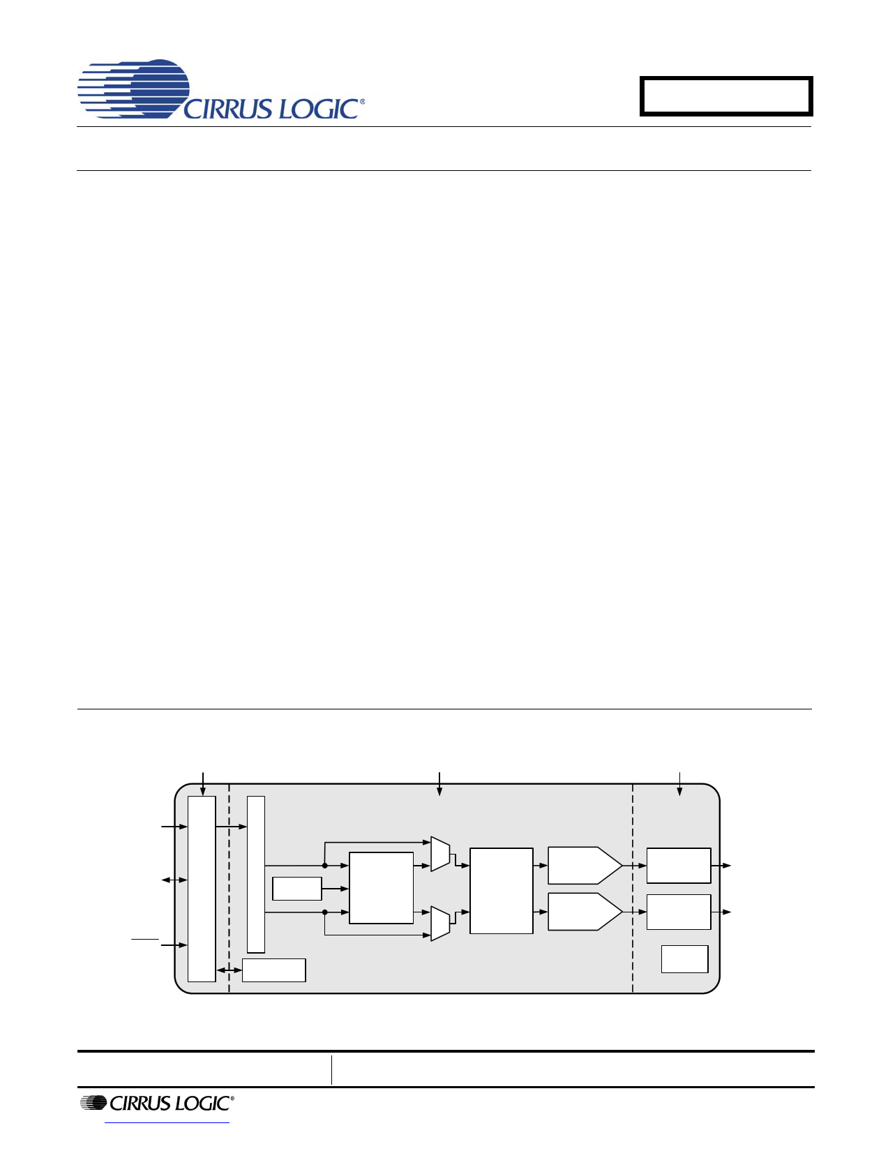
Serial Audio
Input
Hardware
Mode or I2C &
SPI Software
Mode
Control Data
Reset
Beep
Generator
Register
Configuration
Digital
Signal
Processing
Engine
MUX
Switched
Capacitor DAC
Multibit
and Filter
∆Σ Modulator
Switched
Capacitor DAC
MUX
and Filter
Headphone
Amp - GND
Centered
Headphone
Amp - GND
Centered
Charge
Pump
Left HP Out
Right HP Out
Advance Product Information
http://www.cirrus.com
This document contains information for a new product.
Cirrus Logic reserves the right to modify this product without notice.
Copyright © Cirrus Logic, Inc. 2006
(All Rights Reserved)
JULY '06
DS723A1
1 page 
CS43L21
LIST OF FIGURES
Figure 1.Typical Connection Diagram (Software Mode) ............................................................................. 9
Figure 2.Typical Connection Diagram (Hardware Mode) .......................................................................... 10
Figure 3.Headphone Output Test Load ..................................................................................................... 15
Figure 4.Serial Audio Interface Slave Mode Timing .................................................................................. 17
Figure 5.Serial Audio Interface Master Mode Timing ................................................................................ 17
Figure 6.Control Port Timing - I²C ............................................................................................................. 18
Figure 7.Control Port Timing - SPI Format ................................................................................................ 19
Figure 8.Output Architecture ..................................................................................................................... 24
Figure 9.De-Emphasis Curve .................................................................................................................... 25
Figure 10.Beep Configuration Options ...................................................................................................... 26
Figure 11.Peak Detect & Limiter ............................................................................................................... 27
Figure 12.Master Mode Timing ................................................................................................................. 29
Figure 13.Tri-State SCLK/LRCK ............................................................................................................... 30
Figure 14.I²S Format ................................................................................................................................. 30
Figure 15.Left-Justified Format ................................................................................................................. 31
Figure 16.Right-Justified Format (DAC only) ............................................................................................ 31
Figure 17.Initialization Flow Chart ............................................................................................................. 32
Figure 18.Control Port Timing in SPI Mode .............................................................................................. 33
Figure 19.Control Port Timing, I²C Write ................................................................................................... 34
Figure 20.Control Port Timing, I²C Read ................................................................................................... 34
Figure 21.THD+N vs. Output Power per Channel at 1.8 V (16 Ω load) .................................................... 54
Figure 22.THD+N vs. Output Power per Channel at 2.5 V (16 Ω load) .................................................... 54
Figure 23.THD+N vs. Output Power per Channel at 1.8 V (32 Ω load) .................................................... 55
Figure 24.THD+N vs. Output Power per Channel at 2.5 V (32 Ω load) .................................................... 55
Figure 25.Power Dissipation vs. Output Power into Stereo 16 Ω ......................................................................56
Figure 26.Power Dissipation vs. Output Power into Stereo 16 Ω (Log Detail) .......................................... 56
Figure 27.Passband Ripple ....................................................................................................................... 60
Figure 28.Stopband ................................................................................................................................... 60
Figure 29.Transition Band ......................................................................................................................... 60
Figure 30.Transition Band (Detail) ............................................................................................................ 60
LIST OF TABLES
Table 1. I/O Power Rails ............................................................................................................................. 8
Table 2. Hardware Mode Feature Summary ............................................................................................. 23
Table 3. MCLK/LRCK Ratios .................................................................................................................... 29
DS723A1
5
5 Page 
CS43L21
3. CHARACTERISTIC AND SPECIFICATION TABLES
(All Min/Max characteristics and specifications are guaranteed over the Specified Operating Conditions. Typical per-
formance characteristics and specifications are derived from measurements taken at nominal supply voltages and
TA = 25° C.)
SPECIFIED OPERATING CONDITIONS
(AGND=DGND=0 V, all voltages with respect to ground.)
Parameters
Symbol Min Nom Max Units
DC Power Supply (Note 1)
Analog Core
Headphone Amplifier
Digital Core
Serial/Control Port Interface
Ambient Temperature
VA
1.65 1.8 1.89
2.37 2.5 2.63
VA_HP
1.65
2.37
1.8
2.5
1.89
2.63
VD
1.65 1.8 1.89
2.37 2.5 2.63
1.65 1.8 1.89
VL 2.37 2.5 2.63
3.14 3.3 3.47
Commercial - CNZ
Automotive - DNZ
TA
-10 - +70
-40 - +85
V
V
V
V
V
V
V
V
V
°C
°C
ABSOLUTE MAXIMUM RATINGS
(AGND = DGND = 0 V; all voltages with respect to ground.)
Parameters
Symbol
DC Power Supply
Analog VA, VA_HP
Digital
VD
Serial/Control Port Interface
VL
Input Current
(Note 2)
Iin
Digital Input Voltage
(Note 3)
VIND
Ambient Operating Temperature (power applied)
Storage Temperature
TA
Tstg
Min
-0.3
-0.3
-0.3
-
-0.3
-50
-65
Max
3.0
3.0
4.0
±10
VL+ 0.4
+115
+150
Units
V
V
V
mA
V
°C
°C
WARNING: Operation at or beyond these limits may result in permanent damage to the device. Normal operation
is not guaranteed at these extremes.
Notes:
1. The device will operate properly over the full range of the analog, headphone amplifier, digital core and
serial/control port interface supplies.
2. Any pin except supplies. Transient currents of up to ±100 mA on the analog input pins will not cause
SCR latch-up.
3. The maximum over/under voltage is limited by the input current.
DS723A1
11
11 Page | ||
| Páginas | Total 30 Páginas | |
| PDF Descargar | [ Datasheet CDB43L21.PDF ] | |
Hoja de datos destacado
| Número de pieza | Descripción | Fabricantes |
| CDB43L21 | Stereo Digital to Analog Converter | Cirrus Logic |
| Número de pieza | Descripción | Fabricantes |
| SLA6805M | High Voltage 3 phase Motor Driver IC. |
Sanken |
| SDC1742 | 12- and 14-Bit Hybrid Synchro / Resolver-to-Digital Converters. |
Analog Devices |
|
DataSheet.es es una pagina web que funciona como un repositorio de manuales o hoja de datos de muchos de los productos más populares, |
| DataSheet.es | 2020 | Privacy Policy | Contacto | Buscar |