|
|
|
PDF PI74ALVCH16501 Data sheet ( Hoja de datos )
| Número de pieza | PI74ALVCH16501 | |
| Descripción | 18-Bit Universal Bus Transceiver | |
| Fabricantes | Pericom Semiconductor | |
| Logotipo | ||
Hay una vista previa y un enlace de descarga de PI74ALVCH16501 (archivo pdf) en la parte inferior de esta página. Total 5 Páginas | ||
|
No Preview Available !
www.DataSheet4U.com
PI74ALVCH16501
1122334455667788990011223344556677889900112233445566778899001122112233445566778899001122334455667788990011223344556677889900112211223344556677889900112233445566778899001122334455667788990011221122334455667788990011223344556677889900112233445566778899001122112233445566778899001122
18-Bit Universal Bus Transceiver
With 3-State Outputs
Product Features
• PI74ALVCH16501 is designed for low voltage operation
• VCC = 2.3V to 3.6V
• Hysteresis on all inputs
• Typical VOLP (Output Ground Bounce)
< 0.8V at VCC = 3.3V, TA = 25°C
• Typical VOHV (Output VOH Undershoot)
< 2.0V at VCC = 3.3V, TA = 25°C
• Bus Hold retains last active bus state during 3-STATE
eliminating the need for external pullup resistors
• Industrial operation at –40°C to +85°C
• Packages available:
– 48-pin 240 mil wide plastic TSSOP (A)
– 48-pin 300 mil wide plastic SSOP (V)
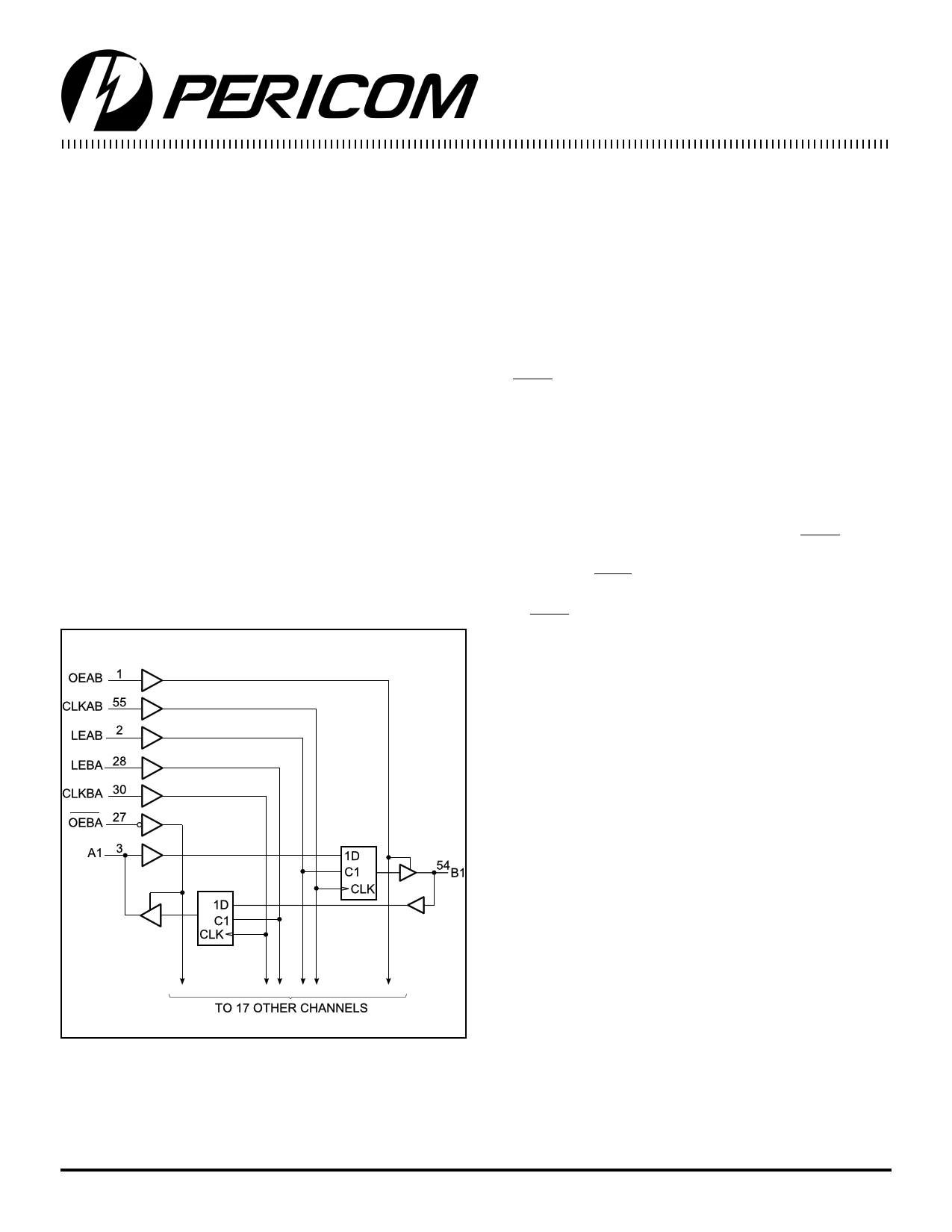
Logic Block Diagram
Product Description
Pericom Semiconductor’s PI74ALVCH series of logic circuits are
produced in the Company’s advanced 0.5 micron CMOS technology,
achieving industry leading speed.
The 18-bit PI74ALVCH16501 univeral bus transceiver is designed
for 2.3V to 3.6V VCC operation.
Data flow in each direction is controlled by Output Enable (OEAB
and OEBA), Latched Enable (LEAB and LEBA), and CLOCK
(CLKAB and CLKBA) inputs. For A-to-B data flow, the device
operates in the transparent mode when LEAB is HIGH. When LEAB
is LOW, the A data is latched if CLKAB is held at a high or low logic
level. If LEAB is LOW, the A-bus is stored in the latch/flip-flop on
the low-to-high transition of CLKAB. When OEAB is HIGH, the
outputs are active. When OEAB is LOW, the outputs are in the high-
impedance state.
Data flow for B to A is similar to that of A to B but uses OEBA, LEBA,
and CLKBA. The Output Enables are complementary (OEAB is
active HIGH and OEBA is active LOW).
To ensure the high-impedance state during power up or power
down, OEBA should be tied to VCC through a pull-up resistor and
OEAB should be tied to GND through a pulldown resistor; the
minimum value of the resistor is determined by the current-sinking
capability of the driver.
Active bus-hold circuitry is provided to hold unused or floating
data inputs at a valid logic level.
1 PS8133A 01/31/00
1 page 
PI74ALVCH16501
123456789012345678901234567890121234567890123456789012345678901212345678901234567189801-2B34I5T678U90N12I1V23E456R78S90A12L34B56U789S01T23R45A678N90S12C12E34I5V67E89R012
Timing Requirements over Operating Range
Parameters
Description
Conditions(1) VCC = 2.5V ± 0.2V
VCC = 2.7V
VCC = 3.3V ± 0.3V
Units
Min. Max. Min. Max. Min. Max.
fCLOCK
Clock frequency
0 150 0 150 0
tW Pulse
Duration
LE high
CLK high or low
3.3 3.3 3.3
3.3 3.3 3.3
tSU Setup
time
Data before CLK ↑
Data before LE ↓, CLK high
Data before LE ↓, CLK low
CL = 50pF
RL = 500Ω
2.2
1.9
1.3
2.1 1.7
1.6 1.5
1.1 1.0
tH Hold
time
Data after CLK ↑
Data after LE ↓ CLK high or low
0.6 0.6 0.7
1.4 1.7 1.4
∆t/∆v(2)
Input Transition Rise or Fall
0 10 0 10 0
Notes:
1. See test circuit and waveforms.
2. Unused control inputs must be held HIGH or LOW to prevent them from floating.
150 MHz
ns
10 ns/V
Switching Characteristics Over Operating Range(1)
Parameters
From
(Input)
To
(Output)
Conditions(1)
VCC = 2.5V ± 0.2V
Min.(2) Max.
VCC = 2.7V VCC = 3.3V ± 0.V
Units
Min.(2) Max. Min.(2) Max.
fMAX
150 150 150 MHz
A or B B or A
1.2 5.4
4.5 1 3.9
tPD LE A or B
1.6 6.3
5.3 1.3 4.6
CLK A or B CL = 50pF
1.7
6.7
tEN OEAB B RL = 500Ω 1.1 6.3
5.6 1.4 4.9
5.3 1.0 4.6 ns
tDIS OEAB B
2.2 6.4
5.7 1.4 5.0
tEN OEBA A
1.4 6.8
6.0 1.1 5.0
tDIS OEBA A
2.0 5.5
Notes:
1. See test circuit and waveforms.
2. Minimum limits are guaranteed but not tested on Propagation Delays.
4.6 1.3 4.2
Operating Characteristics, TA = 25ºC
Parameter
CPD Power Dissipation
Capacitance
Outputs Enabled
Outputs Disabled
Test Conditions
VCC = 2.5V ± 0.2V VCC = 3.3V ± 0.3V
Typical
CL = 50pF, f = 10 MHz
44
6
54
6
Units
pF
Pericom Semiconductor Corporation
2380 Bering Drive • San Jose, CA 95131 • 1-800-435-2336 • Fax (408) 435-1100 • http://www.pericom.com
5 PS8133A 01/31/00
5 Page | ||
| Páginas | Total 5 Páginas | |
| PDF Descargar | [ Datasheet PI74ALVCH16501.PDF ] | |
Hoja de datos destacado
| Número de pieza | Descripción | Fabricantes |
| PI74ALVCH16500 | 18-Bit Universal Bus Transceiver | Pericom Semiconductor |
| PI74ALVCH16501 | 18-Bit Universal Bus Transceiver | Pericom Semiconductor |
| Número de pieza | Descripción | Fabricantes |
| SLA6805M | High Voltage 3 phase Motor Driver IC. |
Sanken |
| SDC1742 | 12- and 14-Bit Hybrid Synchro / Resolver-to-Digital Converters. |
Analog Devices |
|
DataSheet.es es una pagina web que funciona como un repositorio de manuales o hoja de datos de muchos de los productos más populares, |
| DataSheet.es | 2020 | Privacy Policy | Contacto | Buscar |