|
|
|
PDF NTD25P03L Data sheet ( Hoja de datos )
| Número de pieza | NTD25P03L | |
| Descripción | Power MOSFET ( Transistor ) | |
| Fabricantes | ON Semiconductor | |
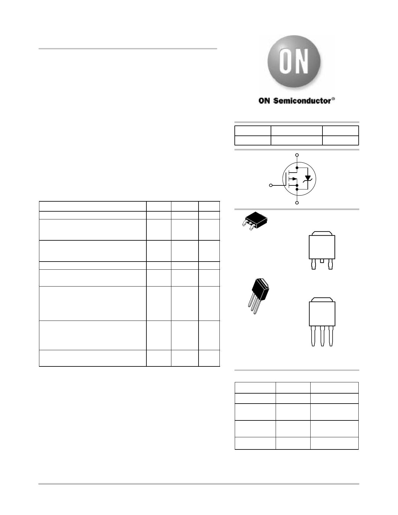
| Logotipo | ||
Hay una vista previa y un enlace de descarga de NTD25P03L (archivo pdf) en la parte inferior de esta página. Total 10 Páginas | ||
|
No Preview Available !
NTD25P03L
Power MOSFET
−25 A, −30 V, Logic Level P−Channel
DPAK
Designed for low voltage, high speed switching applications and to
withstand high energy in the avalanche and commutation modes. The
source−to−drain diode recovery time is comparable to a discrete fast
recovery diode.
Typical Applications
• PWM Motor Controls
• Power Supplies
• Converters
• Bridge Circuits
• Pb−Free Package is Available
MAXIMUM RATINGS (TJ = 25°C unless otherwise noted)
Rating
Symbol Value
Unit
Drain−to−Source Voltage
Gate−to−Source Voltage
− Continuous
− Non−Repetitive (tp ≤ 10 ms)
Drain Current
− Continuous @ TA = 25°C
− Single Pulse (tp ≤ 10 ms)
Total Power Dissipation @ TA = 25°C
Operating and Storage Temperature
Range
VDSS
VGS
VGSM
−30
"15
"20
V
V
Vpk
ID
IDM
PD
TJ, Tstg
−25 A
−w7w5w.DataSheeAt4Up.ckom
75 Watts
−55 to
+150
°C
Single Pulse Drain−to−Source Avalanche
Energy − Starting TJ = 25°C
(VDD = 25 Vdc, VGS = 5.0 Vdc,
Peak IL = 20 Apk, L = 1.0 mH,
RG = 25 W)
Thermal Resistance
− Junction−to−Case
− Junction−to−Ambient (Note 1)
− Junction−to−Ambient (Note 2)
EAS
RqJC
RqJA
RqJA
200 mJ
°C/W
1.65
67
120
Maximum Lead Temperature for Soldering
Purposes, (1/8″ from case for 10 s)
TL
260 °C
Maximum ratings are those values beyond which device damage can occur.
Maximum ratings applied to the device are individual stress limit values (not
normal operating conditions) and are not valid simultaneously. If these limits are
exceeded, device functional operation is not implied, damage may occur and
reliability may be affected.
1. When surface mounted to an FR4 board using 0.5 sq in pad size.
2. When surface mounted to an FR4 board using the minimum recommended
pad size.
© Semiconductor Components Industries, LLC, 2004
August, 2004 − Rev. 1
1
http://onsemi.com
V(BR)DSS
−30 V
RDS(on) TYP
51 mW @ 5.0 V
ID MAX
−25 A
D
P−Channel
G
4
12
3
DPAK
CASE 369C
(Surface Mount)
Style 2
4
S
MARKING DIAGRAMS
4
Drain
1
Gate
2
Drain
3
Source
4
Drain
1
2
3
DPAK
CASE 369D
(Straight Lead)
Style 2
25P03L Device Code
Y = Year
WW = Work Week
12 3
Gate Drain Source
ORDERING INFORMATION
Device
Package
Shipping†
NTD25P03L
NTD25P03LG
NTD25P03L1
DPAK
DPAK
(Pb−Free)
DPAK
Straight Lead
75 Units/Rail
75 Units/Rail
75 Units/Rail
NTD25P03LT4
DPAK
2500/Tape & Reel
†For information on tape and reel specifications,
including part orientation and tape sizes, please
refer to our Tape and Reel Packaging Specification
Brochure, BRD8011/D.
Publication Order Number:
NTD25P03L/D
1 page 
NTD25P03L
10
8 −VDS
QT
30
25
6
Q1
4
20
Q2 −VGS 15
10
2 ID = −25 A 5
TJ = 25°C
Q3
0
0
0 2.5 5 7.5 10 12.5 15
Qg, TOTAL GATE CHARGE (nC)
Figure 8. Gate−to−Source and
Drain−to−Source Voltage versus Total Charge
1000
100
VDD = −15 V
ID = −25 A
VGS = −5.0 V
TJ = 25°C
10
tr
tf
td(off)
td(on)
1
1 10 100
RG, GATE RESISTANCE (W)
Figure 9. Resistive Switching Time Variation
versus Gate Resistance
DRAIN−TO−SOURCE DIODE CHARACTERISTICS
The switching characteristics of a MOSFET body diode
are very important in systems using it as a freewheeling or
commutating diode. Of particular interest are the reverse
recovery characteristics which play a major role in
determining switching losses, radiated noise, EMI and RFI.
System switching losses are largely due to the nature of
the body diode itself. The body diode is a minority carrier
device, therefore it has a finite reverse recovery time, trr, due
to the storage of minority carrier charge, QRR, as shown in
the typical reverse recovery wave form of Figure 14. It is this
stored charge that, when cleared from the diode, passes
through a potential and defines an energy loss. Obviously,
repeatedly forcing the diode through reverse recovery
further increases switching losses. Therefore, one would
like a diode with short trr and low QRR specifications to
minimize these losses.
The abruptness of diode reverse recovery effects the
amount of radiated noise, voltage spikes, and current
ringing. The mechanisms at work are finite irremovable
circuit parasitic inductances and capacitances acted upon by
25
VGS = 0 V
20 TJ = 25°C
high di/dts. The diode’s negative di/dt during ta is directly
controlled by the device clearing the stored charge.
However, the positive di/dt during tb is an uncontrollable
diode characteristic and is usually the culprit that induces
current ringing. Therefore, when comparing diodes, the
ratio of tb/ta serves as a good indicator of recovery
abruptness and thus gives a comparative estimate of
probable noise generated. A ratio of 1 is considered ideal and
values less than 0.5 are considered snappy.
Compared to ON Semiconductor standard cell density
low voltage MOSFETs, high cell density MOSFET diodes
are faster (shorter trr), have less stored charge and a softer
reverse recovery characteristic. The softness advantage of
the high cell density diode means they can be forced through
reverse recovery at a higher di/dt than a standard cell
MOSFET diode without increasing the current ringing or the
noise generated. In addition, power dissipation incurred
from switching the diode will be less due to the shorter
recovery time and lower switching losses.
15
10
5
0
0 0.1 0.2 0.3 0.4 0.5 0.6 0.7 0.8 0.9 1 1.1
−VSD, SOURCE−TO−DRAIN VOLTAGE (VOLTS)
Figure 10. Diode Forward Voltage versus Current
http://onsemi.com
5
5 Page | ||
| Páginas | Total 10 Páginas | |
| PDF Descargar | [ Datasheet NTD25P03L.PDF ] | |
Hoja de datos destacado
| Número de pieza | Descripción | Fabricantes |
| NTD25P03L | Power MOSFET ( Transistor ) | ON Semiconductor |
| Número de pieza | Descripción | Fabricantes |
| SLA6805M | High Voltage 3 phase Motor Driver IC. |
Sanken |
| SDC1742 | 12- and 14-Bit Hybrid Synchro / Resolver-to-Digital Converters. |
Analog Devices |
|
DataSheet.es es una pagina web que funciona como un repositorio de manuales o hoja de datos de muchos de los productos más populares, |
| DataSheet.es | 2020 | Privacy Policy | Contacto | Buscar |