|
|
|
PDF NBSG86ABAEVB Data sheet ( Hoja de datos )
| Número de pieza | NBSG86ABAEVB | |
| Descripción | Evaluation Board Manual | |
| Fabricantes | ON Semiconductor | |
| Logotipo | ||
Hay una vista previa y un enlace de descarga de NBSG86ABAEVB (archivo pdf) en la parte inferior de esta página. Total 20 Páginas | ||
|
No Preview Available !
NBSG86ABAEVB
Evaluation Board Manual
for NBSG86A
http://onsemi.com
EVALUATION BOARD MANUAL
DESCRIPTION
This document describes the NBSG86A evaluation board What measurements can you expect to make?
and the appropriate lab test setups. It should be used in
The following measurements can be performed in the
conjunction with the device data sheet, which includes single–ended (Note 1) or differential mode of operation:
specifications and a full description of device operation.
• Frequency Performance
The board is used to evaluate the NBSG86A
GigaComm™ differential Smart Gate multi-function logic
gate, which can be configured as an AND/NAND,
OR/NOR, XOR/XNOR, or 2:1 MUX. The OLS input of the
NBSG86A is used to program the peak–to–peak output
amplitude between 0 and 800 mV in five discrete steps.
• Output Amplitude (VOH /VOL)
• Output Rise and Fall Time
• Output Skew
• Eye pattern generation
• Jitter
The board is implemented in two layers and provides a
high bandwidth 50 W controlled impedance environment for
• VIHCMR (Input High Common Mode Range)
higher performance. The first layer or primary trace layer is
5 mils thick Rogers RO6002 material, which is engineered
to have equal electrical length on all signal traces from thewww.DataSheet4U.com
NBSG86A device to the sense output. The second layer is
32 mils thick copper ground plane.
For standard lab setup and test, a split (dual) power supply
is required enabling the 50 W impedance from the scope to NOTE:
be used as termination of the ECL signals, where VTT is the
system ground (VCC = 2.0 V, VTT = VCC - 2.0 V and VEE
is -0.5 V or -1.3 V, see Setup 1).
1. Single- ended meas urements can only be made at
VCC - VEE = 3.3 V using this board setup.
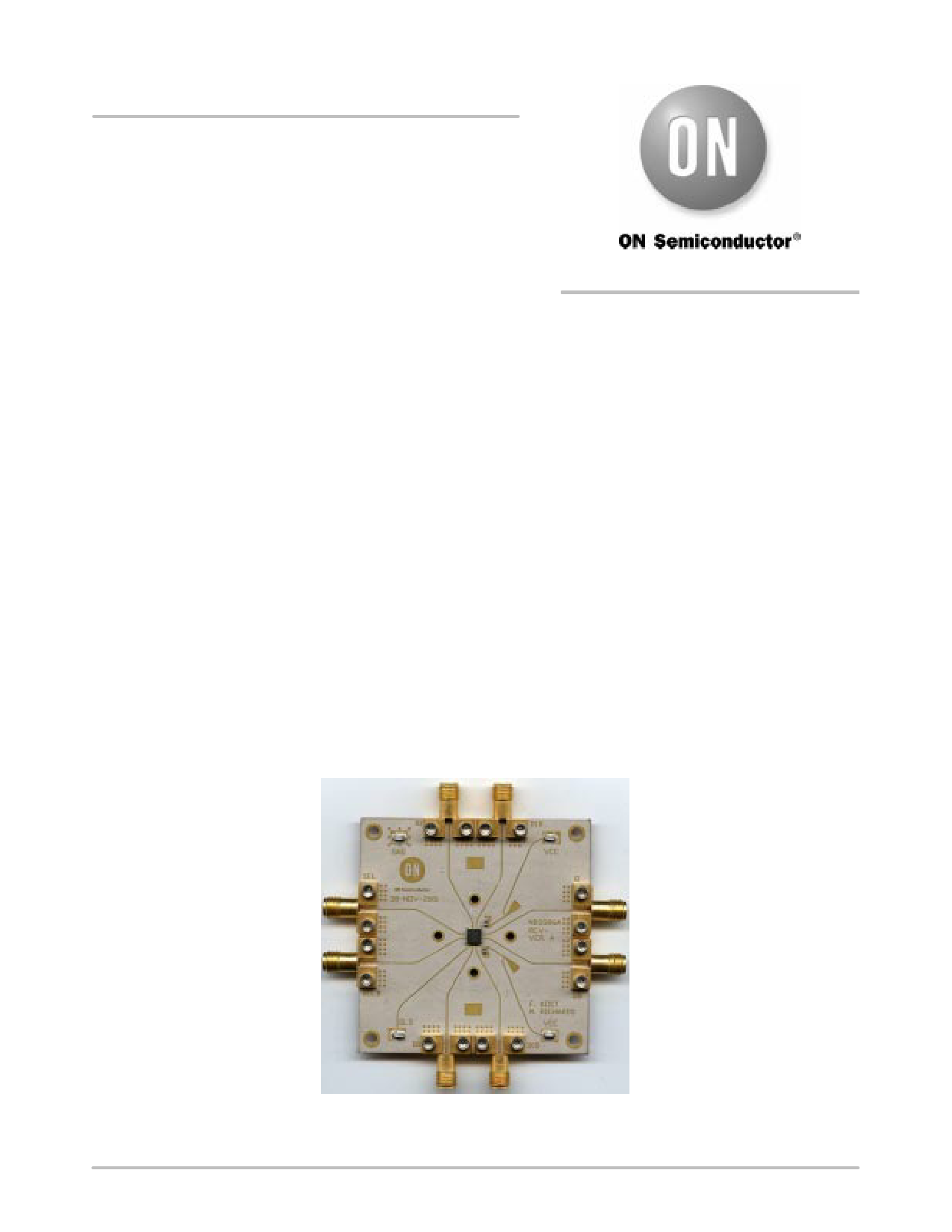
Figure 1. NBSG86A Evaluation Board
© Semiconductor Components Industries, LLC, 2003
March, 2003 - Rev. 0
1
Publication Order Number:
NBSG86ABAEVB/D
1 page 
NBSG86ABAEVB
OR/NOR Function Setup (continued)
Step 2:
Connect the Inputs
For Differential Mode (3.3 V and 2.5 V operation)
2a: Connect the differential outputs of the generator to the differential inputs of the device
(D0/D0 and SEL/SEL).
2a: Connect the D1 input to VTT.
2b: Connect the D1 input to VCC.
2e: Connect the generator trigger to the oscilloscope trigger.
For Single-Ended Mode (3.3 V operation only)
2a: Connect an AC-coupled output of the generator to the desired differential input of the
device.
2b: Connect the unused differential input of the device to VTT (GND) through a 50 W resis-
tor.
2c: Connect the D1 input to VTT.
2d: Connect the D1 input to VCC.
2e: Connect the generator trigger to the oscilloscope trigger.
All Function Setups
Connect OLS (Output Level Select) to the required voltage to obtain desired output
amplitude. Refer to the NBSG86A device data sheet page 2 OLS voltage table.
Step 3:
Setup Input Signal
3a: Set the signal generator amplitude to 400 mV. Note that the signal generator amplitude
can vary from 75 mV to 900 mV to produce a 400 mV DUT output.
3b: Set the signal generator offset to 660 mV (the center of a nominal RSECL output). Note
that the VIHCMR (Input High Voltage Common Mode Range) allows the signal generator
offset to vary as long as VIH is within the VIHCMR range. Refer to the device data sheet for
further information.
3c: Set the generator output for a square wave clock signal with a 50% duty cycle, or for a
PRBS data signal.
Step 4:
Connect Output Signals
4a: Connect the outputs of the evaluation board (Q, Q) to the oscilloscope. The oscilloscope
sampling head must have internal 50 W termination to ground.
NOTE: Where a single output is being used, the unconnected output for the pair must be terminated to
VTT through a 50 W resistor for best operation. Unused pairs may be left unconnected. Since
VTT = 0 V, a standard 50 W SMA termination is recommended.
http://onsemi.com
5
5 Page 
NBSG86ABAEVB
Setup Test Configurations For Differential Operation
Small Signal Setup
Step 2:
Step 3:
Input Setup
2a: Calibrate VNA from 1.0 GHz to 12 GHz.
2b: Set input level to –35 dBm at the output of the 180° Hybrid coupler (input of the DUT).
Output Setup
3a: Set display to measure S21 and record data.
Large Signal Setup
Step 2:
Step 3:
Input Setup
2a: Calibrate VNA from 1.0 GHz to 12 GHz.
2b: Set input levels to -2.0 dBm (500 mV) at the input of DUT.
Output Setup
3a: Set display to measure S21 and record data.
PORT 1
GND
50 W
Rohde & Schwartz
Vector Network Analyzer
PORT 2
1805 Hybrid
Coupler
VCC = 2.0 V
VTT = 0 V
GND D1
SEL
VCC = 2.0 V
D1 VCC
Q
GND
50 W
Bias T
VTT = 0 V
SEL
OLS
D0
Q
D0 VEE
50 W
GND
*See NBSG86A data sheet pg 2.
OLS*
VEE = -1.3 V (3.3 V op)
VTT = 0 V VCC = 2.0 V
Figure 6. NBSG86A Board Setup - Frequency Domain (Differential 2:1 MUX Function - D1 Selected)
http://onsemi.com
11
11 Page | ||
| Páginas | Total 20 Páginas | |
| PDF Descargar | [ Datasheet NBSG86ABAEVB.PDF ] | |
Hoja de datos destacado
| Número de pieza | Descripción | Fabricantes |
| NBSG86ABAEVB | Evaluation Board Manual | ON Semiconductor |
| Número de pieza | Descripción | Fabricantes |
| SLA6805M | High Voltage 3 phase Motor Driver IC. |
Sanken |
| SDC1742 | 12- and 14-Bit Hybrid Synchro / Resolver-to-Digital Converters. |
Analog Devices |
|
DataSheet.es es una pagina web que funciona como un repositorio de manuales o hoja de datos de muchos de los productos más populares, |
| DataSheet.es | 2020 | Privacy Policy | Contacto | Buscar |