|
|
|
PDF WM8956 Data sheet ( Hoja de datos )
| Número de pieza | WM8956 | |
| Descripción | Hi-Fi DAC | |
| Fabricantes | Wolfson Microelectronics | |
| Logotipo | ||
Hay una vista previa y un enlace de descarga de WM8956 (archivo pdf) en la parte inferior de esta página. Total 30 Páginas | ||
|
No Preview Available !
w
WM8956
Hi-Fi DAC with 1W Stereo Class D Speaker Drivers and
Headphone Drivers
DESCRIPTION
FEATURES
The WM8956 is a low power, high quality stereo DAC designed
for portable multimedia applications.
Stereo class D speaker drivers provide 1W per channel into 8
loads with a 5V supply. Low leakage, excellent PSRR and
pop/click suppression mechanisms also allow direct battery
connection to the speaker supply. Flexible speaker boost
settings allow speaker output power to be maximised while
minimising other analogue supply currents.
A highly flexible input configuration for up to three stereo
sources is integrated, with a complete microphone interface.
External component requirements are drastically reduced as no
separate microphone, speaker or headphone amplifiers are
required.
Stereo 24-bit sigma-delta DACs are used with low power over-
sampling digital interpolation filters and a flexible digital audio
interface.
The master clock can be input directly or generated internally by
an onboard PLL, supporting most commonly-used clocking
schemes.
The WM8956 operates at analogue supply voltages down to
2.7V, although the digital supplies can operate at voltages down
to 1.71V to save power. The speaker supply can operate at up
to 5.5V, providing 1W per channel into 8 loads. Unused
functions can be disabled using software control to save power.
The WM8956 is supplied in a very small and thin 5x5mm QFN
package, ideal for use in hand-held and portable systems.
DAC SNR 99dB (‘A’ weighted), THD -87dB at 48kHz, 3.3V
Pop and click suppression
3D Enhancement
Stereo Class D Speaker Driver
- <0.1% THD with 1W per channel into 8 BTL speakers
- 70dB PSRR @217Hz
- 87% efficiency (1W output)
- Flexible internal switching clock
On-chip Headphone Driver
- 40mW output power into 16 at 3.3V
- Capless mode support
- THD+N -70dB at 20mW, SNR 99dB with 16 load
Microphone Interface
- Pseudo differential for high noise immunity
- Integrated low noise MICBIAS
Low Power Consumption
- 16mW headphone playback (2.7V / 1.8V supplies)
Low Supply Voltages
- Analogue 2.7V to 3.6V (Speaker supply up to 5.5V)
- Digital core and I/O: 1.71V to 3.6V
On-chip PLL provides flexible clocking scheme
Sample rates: 8, 11.025, 12, 16, 22.05, 24, 32, 44.1, 48
5x5x0.9mm QFN package
APPLICATIONS
Mobile multimedia
Portable media / DVD players
Games consoles
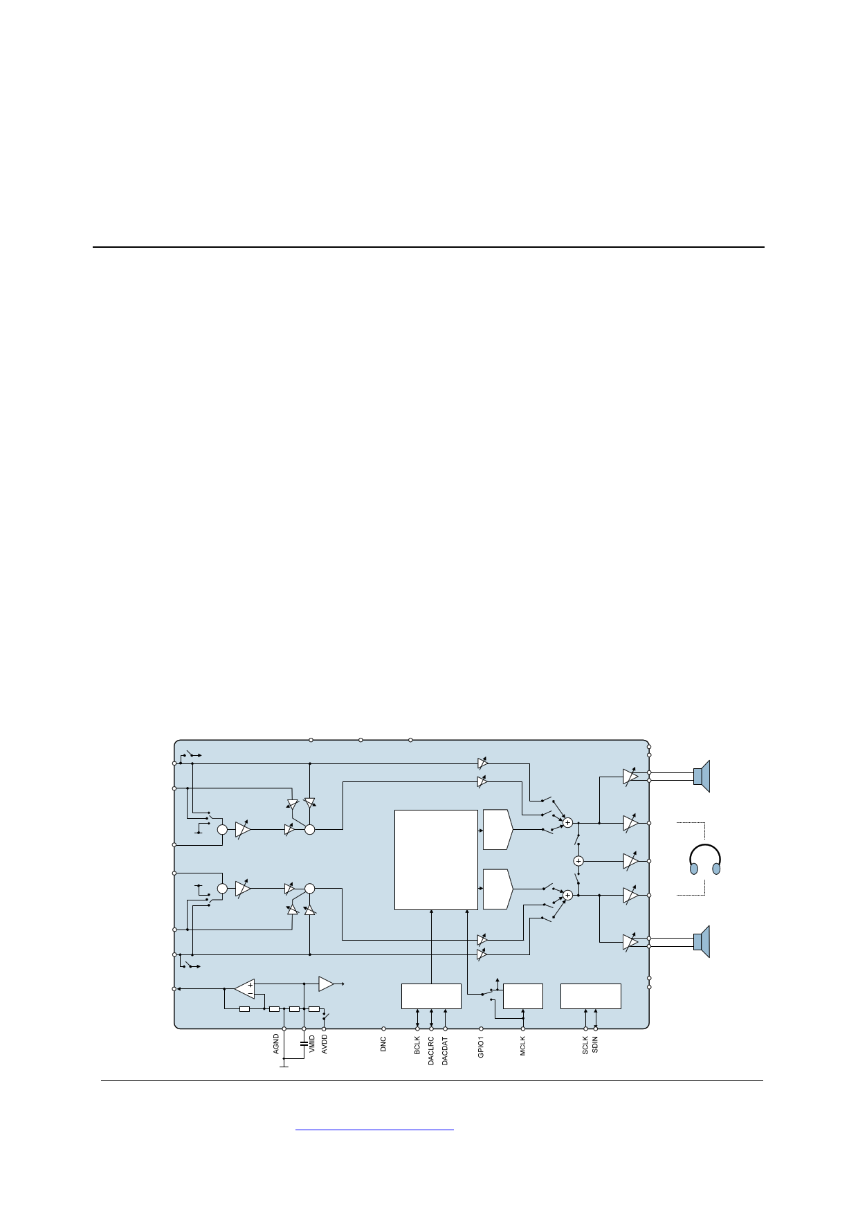
DGND
DCVDD
LINPUT3/
JD2
Jack Detect
LINPUT2
LINPUT1
vmid
RINPUT1
vmid
RINPUT2
-17.25 to +30dB,
0.75dB steps
+
-12 -> 6dB,
3dB steps,
mute
-
0, 13, 20, 29dB, mute
-12 -> 6dB,
3dB steps,
mute
+
INPUT
PGAs
W
WM8956
- 0, 13, 20, 29dB, mute
+
-17.25 to +30dB,
0.75dB steps
-12 -> 6dB,
3dB steps,
mute
+
-12 -> 6dB,
3dB steps,
mute
RINPUT3/
JD3
MICBIAS
Jack Detect
50K 50K
DACREF
DBVDD
0 to -21dB,
3dB steps
0 to -21dB,
3dB steps
DAC DIGITAL FILTERS
DE-EMPHASIS
3D ENHANCE
VOLUME
DAC
DAC
DIGITAL AUDIO
INTERFACE
A-law and u-law support
0 to -21dB,
3dB steps
0 to -21dB,
3dB steps
GPIO1
PLL
LEFT
MIXER
MONO
MIXER
CLASS D
SPKVDD1
SPKVDD2
SPK_LP
-73 to 6dB
1dB steps,
mute
+BOOST
SPK_LN
-73 to 6dB
1dB steps,
mute
0dB / -6dB
HP_L
OUT3
RIGHT
MIXER
HP_R
-73 to 6dB
1dB steps,
mute
CLASS D
SPK_RN
CONTROL
INTERFACE
-73 to 6dB
1dB steps,
mute
+BOOST
SPK_RP
SPKGND1
SPKGND2
WOLFSON MICROELECTRONICS plc
To receive regular email updates, sign up at http://www.wolfsonmicro.com/enews
Production Data, November 2011, Rev 4.1
Copyright 2011 Wolfson Microelectronics plc
1 page 
Production Data
WM8956
ABSOLUTE MAXIMUM RATINGS
Absolute Maximum Ratings are stress ratings only. Permanent damage to the device may be caused by continuously
operating at or beyond these limits. Device functional operating limits and guaranteed performance specifications are given
under Electrical Characteristics at the test conditions specified.
ESD Sensitive Device. This device is manufactured on a CMOS process. It is therefore generically susceptible
to damage from excessive static voltages. Proper ESD precautions must be taken during handling and storage
of this device.
Wolfson tests its package types according to IPC/JEDEC J-STD-020B for Moisture Sensitivity to determine acceptable storage
conditions prior to surface mount assembly. These levels are:
MSL1 = unlimited floor life at <30C / 85% Relative Humidity. Not normally stored in moisture barrier bag.
MSL2 = out of bag storage for 1 year at <30C / 60% Relative Humidity. Supplied in moisture barrier bag.
MSL3 = out of bag storage for 168 hours at <30C / 60% Relative Humidity. Supplied in moisture barrier bag.
The Moisture Sensitivity Level for each package type is specified in Ordering Information.
CONDITION
Supply voltages (excluding SPKVDD1 and SPKVDD2)
SPKVDD1, SPKVDD2
Voltage range digital inputs
Voltage range analogue inputs
Operating temperature range, TA
Storage temperature after soldering
MIN
-0.3V
-0.3V
DGND -0.3V
AGND -0.3V
-40C
-65C
MAX
+4.5V
+7V
DBVDD +0.3V
AVDD +0.3V
+85C
+150C
Notes:
1. Analogue, digital and speaker grounds must always be within 0.3V of each other.
2. All digital and analogue supplies are completely independent from each other (i.e. not internally connected).
3. DCVDD must be less than or equal to AVDD and DBVDD.
4. AVDD must be less than or equal to SPKVDD1 and SPKVDD2.
5. SPKVDD1 and SPKVDD2 must be high enough to support the peak output voltage when using DCGAIN and ACGAIN
functions, to avoid output waveform clipping. Peak output voltage is AVDD*(DCGAIN+ACGAIN)/2.
RECOMMENDED OPERATING CONDITIONS
PARAMETER
Digital supply range (Core)
Digital supply range (Buffer)
Analogue supplies range
Speaker supply range
Ground
SYMBOL
DCVDD
DBVDD
AVDD
SPKVDD1, SPKVDD2
DGND, AGND, SPKGND1,
SPKGND2
MIN
1.71
1.71
2.7
2.7
TYP
0
MAX
3.6
3.6
3.6
5.5
UNIT
V
V
V
V
V
w
PD, November 2011, Rev 4.1
5
5 Page 
Production Data
SIGNAL TIMING REQUIREMENTS
SYSTEM CLOCK TIMING
WM8956
MCLK
tMCLKY
Figure 2 System Clock Timing Requirements
Test Conditions
DCVDD=1.8V, DBVDD=AVDD=SPKVDD1=SPKVDD2=3.3V, DGND=AGND=SPKGND1=SPKGND2=0V, TA = +25oC
PARAMETER
System Clock Timing Information
MCLK cycle time
MCLK duty cycle
SYMBOL
TMCLKY
TMCLKDS
CONDITIONS
MIN
33.33
60:40
TYP
MAX
40:60
UNIT
ns
AUDIO INTERFACE TIMING – MASTER MODE
Figure 2 Digital Audio Data Timing – Master Mode (see Control Interface)
w
PD, November 2011, Rev 4.1
11
11 Page | ||
| Páginas | Total 30 Páginas | |
| PDF Descargar | [ Datasheet WM8956.PDF ] | |
Hoja de datos destacado
| Número de pieza | Descripción | Fabricantes |
| WM8950 | ADC WITH MICROPHONE INPUT AND PROGRAMMABLE DIGITAL FILTERS | Wolfson Microelectronics plc |
| WM8951L | Stereo ADC with Microphone Input and Clock Generator | Wolfson Microelectronics plc |
| WM8955 | STEREO DAC FOR PORTABLE AUDIO APPLICATIONS | Wolfson Microelectronics plc |
| WM8955BL | Stereo DAC | Wolfson Microelectronics |
| Número de pieza | Descripción | Fabricantes |
| SLA6805M | High Voltage 3 phase Motor Driver IC. |
Sanken |
| SDC1742 | 12- and 14-Bit Hybrid Synchro / Resolver-to-Digital Converters. |
Analog Devices |
|
DataSheet.es es una pagina web que funciona como un repositorio de manuales o hoja de datos de muchos de los productos más populares, |
| DataSheet.es | 2020 | Privacy Policy | Contacto | Buscar |