|
|
|
PDF NCP5208 Data sheet ( Hoja de datos )
| Número de pieza | NCP5208 | |
| Descripción | DDR-I/II Termination Regulator | |
| Fabricantes | ON Semiconductor | |
| Logotipo | ||
Hay una vista previa y un enlace de descarga de NCP5208 (archivo pdf) en la parte inferior de esta página. Total 9 Páginas | ||
|
No Preview Available !
NCP5208
DDR−I/II Termination
Regulator
The NCP5208 is a linear regulator specifically designed for the
active termination of DDR−I/II SDRAM. The device can be operated
from a single supply voltage as low as 1.7 V. For DDR−I
applications, the device is capable of sourcing and sinking current up
to 1.5 A with the output voltage regulated to within "3% or better. A
separate voltage feedback pin ensures superior load regulation
against load and line changes.
Protective features include soft−start, source/sink current limits
and thermal shutdown. Open−drain VTT OK output (POK) is added
for system monitoring. The shutdown pin can tri−state the regulator
output for Suspend To RAM (STR) state. This device is available in a
SOIC−8 package.
Features
• Supports Both DDR−I and DDR−II SDRAM Requirements
• Single Supply Voltage Operation as Low as 1.7 V
• Integrated Power MOSFETs
• Few External Components Needed
• Source and Sink Current Up to 1.5 A
• Load Regulation Within "3%
• Both Source and Sink Current Limits
• Open−Drain VTT OK (POK) Pin
www.DataSheet4U.com
• Shutdown Pin
• Thermal Shutdown
• Housed in SOIC−8 Package
• Pb−Free Package is Available
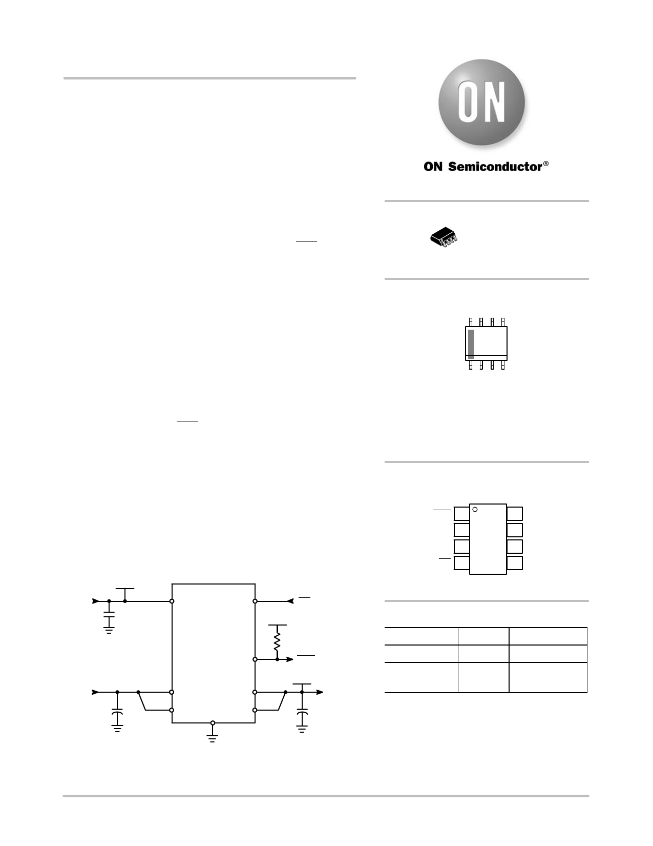
Typical Applications
• DDR Termination Voltage
• Active Bus Termination (SSTL−2, SSTL−3)
2.5 V
VDDQ
VDDQ
SD
AVIN
2.5 V
CIN
AVIN
PVIN
NCP5208
POK
VTT
VTT 1.25 V,
VFB
1.5 A
COUT
GND
Figure 1. Typical Application Circuit
http://onsemi.com
SOIC−8
D SUFFIX
1 CASE 751
MARKING DIAGRAM
8
N5208
ALYW
G
1
A = Assembly Location
L = Wafer Lot
Y = Year
W = Work Week
G = Pb−Free Package
PIN CONNECTIONS
POK 1
GND 2
VFB 3
SD 4
8 VTT
7 PVIN
6 AVIN
5 VDDQ
(Top View)
ORDERING INFORMATION
Device
Package
Shipping†
NCP5208DR2
NCP5208DR2G
SOIC−8
SOIC−8
(Pb−Free)
2500/Tape & Reel
2500/Tape & Reel
†For information on tape and reel specifications,
including part orientation and tape sizes, please
refer to our Tape and Reel Packaging Specifications
Brochure, BRD8011/D.
© Semiconductor Components Industries, LLC, 2006
May, 2006 − Rev. 5
1
Publication Order Number:
NCP5208/D
1 page 
NCP5208
TYPICAL OPERATING CHARACTERISTICS
55
52
49
0.4 ms ON, 1.6 ms OFF
46
43 PVIN = AVIN = VDDQ = 2.5 V
IVTT = 0 A
40
0 10 20 30 40 50 60 70
TA, AMBIENT TEMPERATURE (°C)
Figure 9. VDDQ Input Impedance vs. Ambient
Temperature
TYPICAL OPERATING WAVEFORMS
0.4 ms ON, 1.6 ms OFF
(PVIN = AVIN = VDDQ = 1.8 V)
Upper Trace: VTT Output Waveform, 50 mV/Division, AC Coupled
Lower Trace: Loading Current, IVTT, 500 mA/Division
Figure 10. VTT Current Source Transient
(PVIN = AVIN = VDDQ = 1.8 V)
Upper Trace: VTT Output Waveform, 50 mV/Division, AC Coupled
Lower Trace: Loading Current, IVTT, 500 mA/Division
Figure 11. VTT Current Sink Transient
0.4 ms ON, 1.6 ms OFF
0.4 ms ON, 1.6 ms OFF
(PVIN = AVIN = VDDQ = 2.5 V)
Upper Trace: VTT Output Waveform, 50 mV/Division, AC Coupled
Lower Trace: Loading Current, IVTT, 1 A/Division
Figure 12. VTT Current Source Transient
(PVIN = AVIN = VDDQ = 2.5 V)
Upper Trace: VTT Output Waveform, 50 mV/Division, AC Coupled
Lower Trace: Loading Current, IVTT, 1 A/Division
Figure 13. VTT Current Sink Transient
http://onsemi.com
5
5 Page | ||
| Páginas | Total 9 Páginas | |
| PDF Descargar | [ Datasheet NCP5208.PDF ] | |
Hoja de datos destacado
| Número de pieza | Descripción | Fabricantes |
| NCP5201 | Dual Output DDR Power Controller | ON Semiconductor |
| NCP5203 | 2-in-1 DDR Power Controller | ON |
| NCP5203MNR2 | 2-in-1 DDR Power Controller | ON |
| NCP5203MNR2G | 2-in-1 DDR Power Controller | ON |
| Número de pieza | Descripción | Fabricantes |
| SLA6805M | High Voltage 3 phase Motor Driver IC. |
Sanken |
| SDC1742 | 12- and 14-Bit Hybrid Synchro / Resolver-to-Digital Converters. |
Analog Devices |
|
DataSheet.es es una pagina web que funciona como un repositorio de manuales o hoja de datos de muchos de los productos más populares, |
| DataSheet.es | 2020 | Privacy Policy | Contacto | Buscar |