|
|
|
PDF CA3130A Data sheet ( Hoja de datos )
| Número de pieza | CA3130A | |
| Descripción | 15Mhz BiMOS Operational Amplifier | |
| Fabricantes | Intersil | |
| Logotipo | ||
Hay una vista previa y un enlace de descarga de CA3130A (archivo pdf) en la parte inferior de esta página. Total 17 Páginas | ||
|
No Preview Available !
®
Data Sheet
CA3130, CA3130A
August 1, 2005
FN817.6
15MHz, BiMOS Operational Amplifier with
MOSFET Input/CMOS Output
CA3130A and CA3130 are op amps that combine the
advantage of both CMOS and bipolar transistors.
Gate-protected P-Channel MOSFET (PMOS) transistors are
used in the input circuit to provide very-high-input
impedance, very-low-input current, and exceptional speed
performance. The use of PMOS transistors in the input stage
results in common-mode input-voltage capability down to
0.5V below the negative-supply terminal, an important
attribute in single-supply applications.
A CMOS transistor-pair, capable of swinging the output
voltage to within 10mV of either supply-voltage terminal (at
very high values of load impedance), is employed as the
output circuit.
The CA3130 Series circuits operate at supply voltages
ranging from 5V to 16V, (±2.5V to ±8V). They can be phase
compensated with a single external capacitor, and have
terminals for adjustment of offset voltage for applications
requiring offset-null capability. Terminal provisions are also
made to permit strobing of the output stage.
• The CA3130A offers superior input characteristics over
those of the CA3130.
Ordering Information
PART NO.
(BRAND)
TEMP.
RANGE (oC)
PACKAGE
PKG.
DWG. #
CA3130AE
-55 to 125 8 Ld PDIP
E8.3
CA3130AM
(3130A)
-55 to 125 8 Ld SOIC
M8.15
CA3130AM96
(3130A)
-55 to 125 8 Ld SOIC
Tape and Reel
M8.15
CA3130AMZ
-55 to 125 8 Ld SOIC
(3130AZ) (Note)
(Pb-free)
M8.15
CA3130AMZ96
-55 to 125 8 Ld SOIC
M8.15
(3130AZ) (Note)
Tape and Reel (Pb-free)
CA3130E
-55 to 125 8 Ld PDIP
E8.3
CA3130EZ
(Note)
-55 to 125 8 Ld PDIP*
(Pb-free)
E8.3
CA3130M
(3130)
-55 to 125 8 Ld SOIC
M8.15
CA3130M96
(3130)
-55 to 125 8 Ld SOIC
Tape and Reel
M8.15
CA3130MZ
-55 to 125 8 Ld SOIC
(3130MZ) (Note)
(Pb-free)
M8.15
CA3130MZ96
(3130MZ)
-55 to 125 8 Ld SOIC
M8.15
Tape and Reel (Pb-free)
*Pb-free PDIPs can be used for through hole wave solder processing only. They are not
intended for use in Reflow solder processing applications.
NOTE: Intersil Pb-free plus anneal products employ special Pb-free material sets;
molding compounds/die attach materials and 100% matte tin plate termination finish,
which are RoHS compliant and compatible with both SnPb and Pb-free soldering
operations. Intersil Pb-free products are MSL classified at Pb-free peak reflow
temperatures that meet or exceed the Pb-free requirements of IPC/JEDEC J STD-020.
Features
• MOSFET Input Stage Provides:
- Very High ZI = 1.5 TΩ (1.5 x 10¹²Ω) (Typ)
- Very Low II . . . . . . . . . . . . . 5pA (Typ) at 15V Operation
. . . . . . . . . . . . . . . . . . . . . .= 2pA (Typ) at 5V Operation
• Ideal for Single-Supply Applications
• Common-Mode Input-Voltage Range Includes
Negative Supply Rail; Input Terminals can be Swung 0.5V
Below Negative Supply Rail
• CMOS Output Stage Permits Signal Swing to Either (or
both) Supply Rails
• Pb-Free Plus Anneal Available (RoHS Compliant)
Applications
• Ground-Referenced Single Supply Amplifiers
• Fast Sample-Hold Amplifiers
• Long-Duration Timers/Monostables
• High-Input-Impedance Comparators
(Ideal Interface with Digital CMOS)
• High-Input-Impedance Wideband Amplifiers
• Voltage Followers (e.g. Follower for Single-Supply D/A
Converter)
• Voltage Regulators (Permits Control of Output Voltage
Down to 0V)
• Peak Detectors
• Single-Supply Full-Wave Precision Rectifiers
• Photo-Diode Sensor Amplifiers
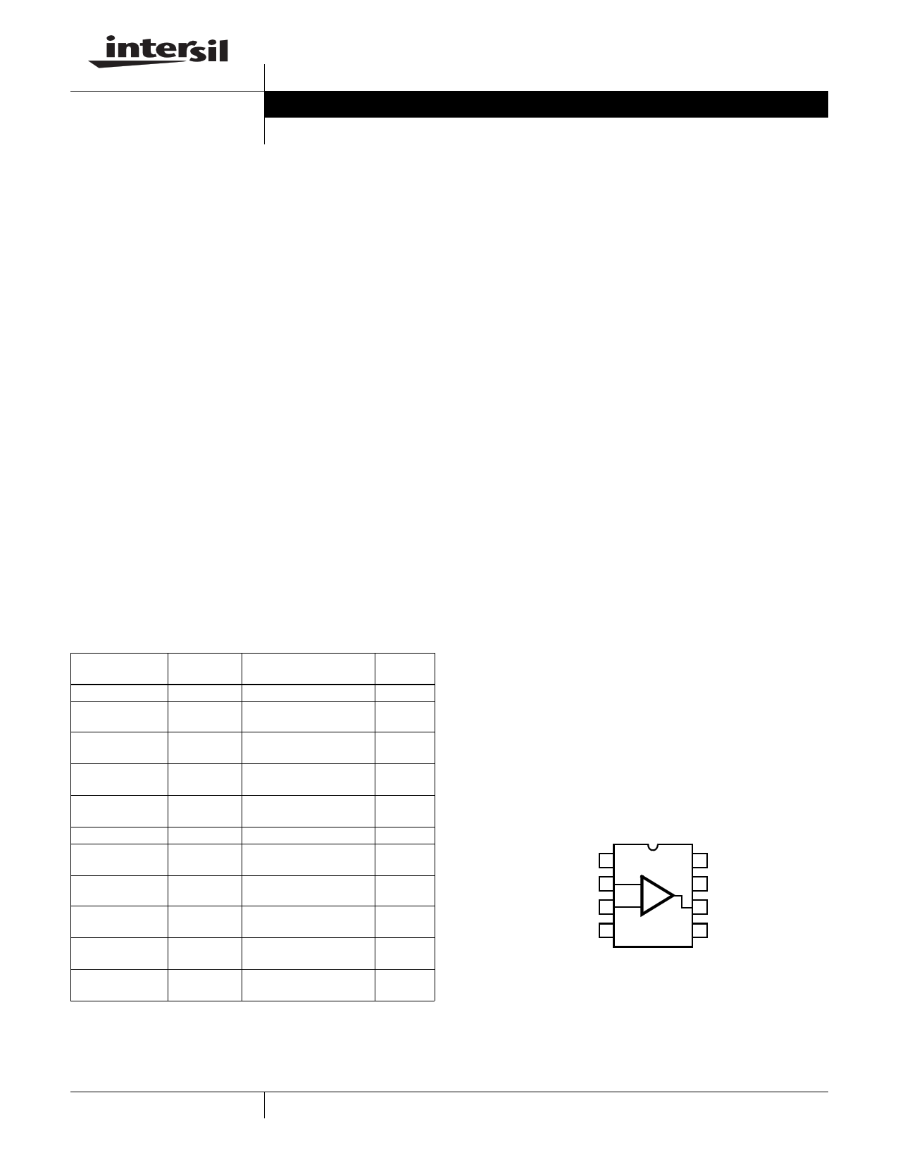
Pinout
CA3130, CA3130A
(PDIP, SOIC)
TOP VIEW
OFFSET
NULL
INV.
INPUT
NON-INV.
INPUT
1
2
3
V- 4
-
+
8 STROBE
7 V+
6 OUTPUT
5 OFFSET
NULL
1
CAUTION: These devices are sensitive to electrostatic discharge; follow proper IC Handling Procedures.
1-888-INTERSIL or 1-888-468-3774 | Intersil (and design) is a registered trademark of Intersil Americas Inc.
Copyright Intersil Americas Inc. 2002, 2005. All Rights Reserved
All other trademarks mentioned are the property of their respective owners.
1 page 
CA3130, CA3130A
CA3130
200µA 1.35mA
BIAS CKT.
200µA
8mA
(NOTE 5)
0mA
(NOTE 7)
V+
7
+
3
INPUT
2
-
AV ≈ 5X
AV ≈
6000X
AV ≈
30X
OUTPUT
6
V-
4
51
OFFSET
NULL
NOTES:
CC
COMPENSATION
(WHEN REQUIRED)
8
STROBE
6. Total supply voltage (for indicated voltage gains) = 15V with input
terminals biased so that Terminal 6 potential is +7.5V above
Terminal 4.
7. Total supply voltage (for indicated voltage gains) = 15V with
output terminal driven to either supply rail.
FIGURE 1. BLOCK DIAGRAM OF THE CA3130 SERIES
Cascade-connected PMOS transistors Q2, Q4 are the
constant-current source for the input stage. The biasing circuit
for the constant-current source is subsequently described.
The small diodes D5 through D8 provide gate-oxide protection
against high-voltage transients, including static electricity
during handling for Q6 and Q7.
Second-Stage
Most of the voltage gain in the CA3130 is provided by the
second amplifier stage, consisting of bipolar transistor Q11
and its cascade-connected load resistance provided by
PMOS transistors Q3 and Q5. The source of bias potentials
for these PMOS transistors is subsequently described. Miller
Effect compensation (roll-off) is accomplished by simply
connecting a small capacitor between Terminals 1 and 8. A
47pF capacitor provides sufficient compensation for stable
unity-gain operation in most applications.
Bias-Source Circuit
At total supply voltages, somewhat above 8.3V, resistor R2
and zener diode Z1 serve to establish a voltage of 8.3V across
the series-connected circuit, consisting of resistor R1, diodes
D1 through D4, and PMOS transistor Q1. A tap at the junction
of resistor R1 and diode D4 provides a gate-bias potential of
about 4.5V for PMOS transistors Q4 and Q5 with respect to
Terminal 7. A potential of about 2.2V is developed across
diode-connected PMOS transistor Q1 with respect to Terminal
7 to provide gate bias for PMOS transistors Q2 and Q3. It
should be noted that Q1 is “mirror-connected (see Note 8)” to
both Q2 and Q3. Since transistors Q1, Q2, Q3 are designed to
be identical, the approximately 200µA current in Q1
establishes a similar current in Q2 and Q3 as constant current
sources for both the first and second amplifier stages,
respectively.
At total supply voltages somewhat less than 8.3V, zener
diode Z1 becomes nonconductive and the potential,
developed across series-connected R1, D1-D4, and Q1,
varies directly with variations in supply voltage.
Consequently, the gate bias for Q4, Q5 and Q2, Q3 varies in
accordance with supply-voltage variations. This variation
results in deterioration of the power-supply-rejection ratio
(PSRR) at total supply voltages below 8.3V. Operation at
total supply voltages below about 4.5V results in seriously
degraded performance.
Output Stage
The output stage consists of a drain-loaded inverting
amplifier using CMOS transistors operating in the Class A
mode. When operating into very high resistance loads, the
output can be swung within millivolts of either supply rail.
Because the output stage is a drain-loaded amplifier, its gain
is dependent upon the load impedance. The transfer
characteristics of the output stage for a load returned to the
negative supply rail are shown in Figure 2. Typical op amp
loads are readily driven by the output stage. Because large-
signal excursions are non-linear, requiring feedback for good
waveform reproduction, transient delays may be
encountered. As a voltage follower, the amplifier can achieve
0.01% accuracy levels, including the negative supply rail.
NOTE:
8. For general information on the characteristics of CMOS
transistor-pairs in linear-circuit applications, see File Number
619, data sheet on CA3600E “CMOS Transistor Array”.
17.5
SUPPLY VOLTAGE: V+ = 15, V- = 0V
15 TA = 25oC
LOAD RESISTANCE = 5kΩ
12.5
10
2kΩ
1kΩ
500Ω
7.5
5
2.5
0
0 2.5 5 7.5 10 12.5 15 17.5 20 22.5
GATE VOLTAGE (TERMINALS 4 AND 8) (V)
FIGURE 2. VOLTAGE TRANSFER CHARACTERISTICS OF
CMOS OUTPUT STAGE
5
5 Page 
CA3130, CA3130A
6VP-P INPUT;
BW (-3dB) = 1.3MHz
0.3VP-P INPUT;
BW (-3dB) = 240kHz
10kΩ
3
2
+7.5V
7
+
CA3130
-
4
0.01µF
6
1N914
100
kΩ
0.01µF
+DC
OUTPUT
+
5µF
-
2kΩ -7.5V
6VP-P INPUT;
BW (-3dB) = 360kHz
0.3VP-P INPUT;
BW (-3dB) = 320kHz
10kΩ
3
2
+7.5V
7
+
CA3130
-
4
0.01µF
6
1N914
100
kΩ
0.01µF
-DC
OUTPUT
-
5µF
+
2kΩ -7.5V
FIGURE 12A. PEAK POSITIVE DETECTOR CIRCUIT
FIGURE 12B. PEAK NEGATIVE DETECTOR CIRCUIT
FIGURE 12. PEAK-DETECTOR CIRCUITS
CURRENT
LIMIT
ADJ
3Ω
R2
1kΩ
+
IC3 1kΩ
CA3086
Q5 13
10 7 3
12 14
Q4 Q3 Q2 Q1
962 4
11 8 1 5
+
+20V
INPUT
-
390Ω
0.01µF
2.2kΩ
+
IC2 - 25µF
CA3086 10 11 1, 2
Q4
9
Q1
3
8, 7 5
Q3
6
Q2
4
Q5 14
12
13
R1
50kΩ
62kΩ
20kΩ
1kΩ
56pF
ERROR
1 AMPLIFIER
8
7
-2
6 CA3130
IC1 + 3
4
100kΩ
VOLTAGE
ADJUST
0.01
µF
OUTPUT
0 TO 13V
AT
40mA
5µF +
25V -
30kΩ
-
REGULATION (NO LOAD TO FULL LOAD): <0.01%
INPUT REGULATION: 0.02%/V
HUM AND NOISE OUTPUT: <25µV UP TO 100kHz
FIGURE 13. VOLTAGE REGULATOR CIRCUIT (0V TO 13V AT 40mA)
11
11 Page | ||
| Páginas | Total 17 Páginas | |
| PDF Descargar | [ Datasheet CA3130A.PDF ] | |
Hoja de datos destacado
| Número de pieza | Descripción | Fabricantes |
| CA3130 | 15Mhz BiMOS Operational Amplifier | Intersil |
| CA3130 | High Rellablilty BiMOS Operational Amplifiers | RCA Solid State |
| CA3130 | BiMOS Operational Amplifiers | General Electric Solid State |
| CA3130 | Operational Amplifiers | Thomson |
| Número de pieza | Descripción | Fabricantes |
| SLA6805M | High Voltage 3 phase Motor Driver IC. |
Sanken |
| SDC1742 | 12- and 14-Bit Hybrid Synchro / Resolver-to-Digital Converters. |
Analog Devices |
|
DataSheet.es es una pagina web que funciona como un repositorio de manuales o hoja de datos de muchos de los productos más populares, |
| DataSheet.es | 2020 | Privacy Policy | Contacto | Buscar |