|
|
|
PDF HI7191 Data sheet ( Hoja de datos )
| Número de pieza | HI7191 | |
| Descripción | Sigma Delta A/D Converter | |
| Fabricantes | Intersil Corporation | |
| Logotipo | ||
Hay una vista previa y un enlace de descarga de HI7191 (archivo pdf) en la parte inferior de esta página. Total 24 Páginas | ||
|
No Preview Available !
HI7191
March 1998
24-Bit, High Precision,
Sigma Delta A/D Converter
Features
• 22-Bit Resolution with No Missing Code
• 0.0007% Integral Non-Linearity (Typ)
• 20mV to ±2.5V Full Scale Input Ranges
• Internal PGIA with Gains of 1 to 128
• Serial Data I/O Interface, SPI Compatible
• Differential Analog and Reference Inputs
• Internal or System Calibration
• -120dB Rejection of 60/50Hz Line Noise
• Settling Time of 4 Conversions (Max) for a Step Input
Applications
• Process Control and Measurement
• Industrial Weight Scales
• Part Counting Scales
• Laboratory Instrumentation
• Seismic Monitoring
• Magnetic Field Monitoring
• Additional Reference Literature
- TB348 “HI7190/1 Negative Full Scale Error vs
Conversion Frequency”
- AN9504 “A Brief Intro to Sigma Delta Conversion”
- TB329 “Intersil Sigma Delta Calibration Technique”
- AN9505 “Using the HI7190 Evaluation Kit”
- TB331 “Using the HI7190 Serial Interface”
- AN9527 “Interfacing HI7190 to a Microcontroller”
- AN9532 “Using HI7190 in a Multiplexed System”
- AN9601 “Using HI7190 with a Single +5V Supply”
Description
The Intersil HI7191 is a monolithic instrumentation, sigma delta
A/D converter which operates from ±5V supplies. Both the sig-
nal and reference inputs are fully differential for maximum flexi-
bility and performance. An internal Programmable Gain
Instrumentation Amplifier (PGIA) provides input gains from 1 to
128 eliminating the need for external pre-amplifiers. The on-
demand converter auto-calibrate function is capable of remov-
ing offset and gain errors existing in external and internal cir-
cuitry. The on-board user programmable digital filter provides
over -120dB of 60/50Hz noise rejection and allows fine tuning
of resolution and conversion speed over a wide dynamic range.
The HI7191 and HI7191 are functionally the same device so all
discussion will refer to the HI7191 for simplicity.
The HI7191 contains a serial I/O port and is compatible with
most synchronous transfer formats including both the Motor-
ola 6805/11 series SPI and Intel 8051 series SSR protocols.
A sophisticated set of commands gives the user control over
calibration, PGIA gain, device selection, standby mode, and
several other features. The On-chip Calibration Registers
allow the user to read and write calibration data.
Ordering Information
TEMP.
PART NUMBER RANGE (oC)
PACKAGE
HI7191IP
-40 to 85 20 Ld PDIP
HI7191IB
-40 to 85 20 Ld SOIC
HI7190EVAL
Evaluation Kit
PKG.
NO.
E20.3
M20.3
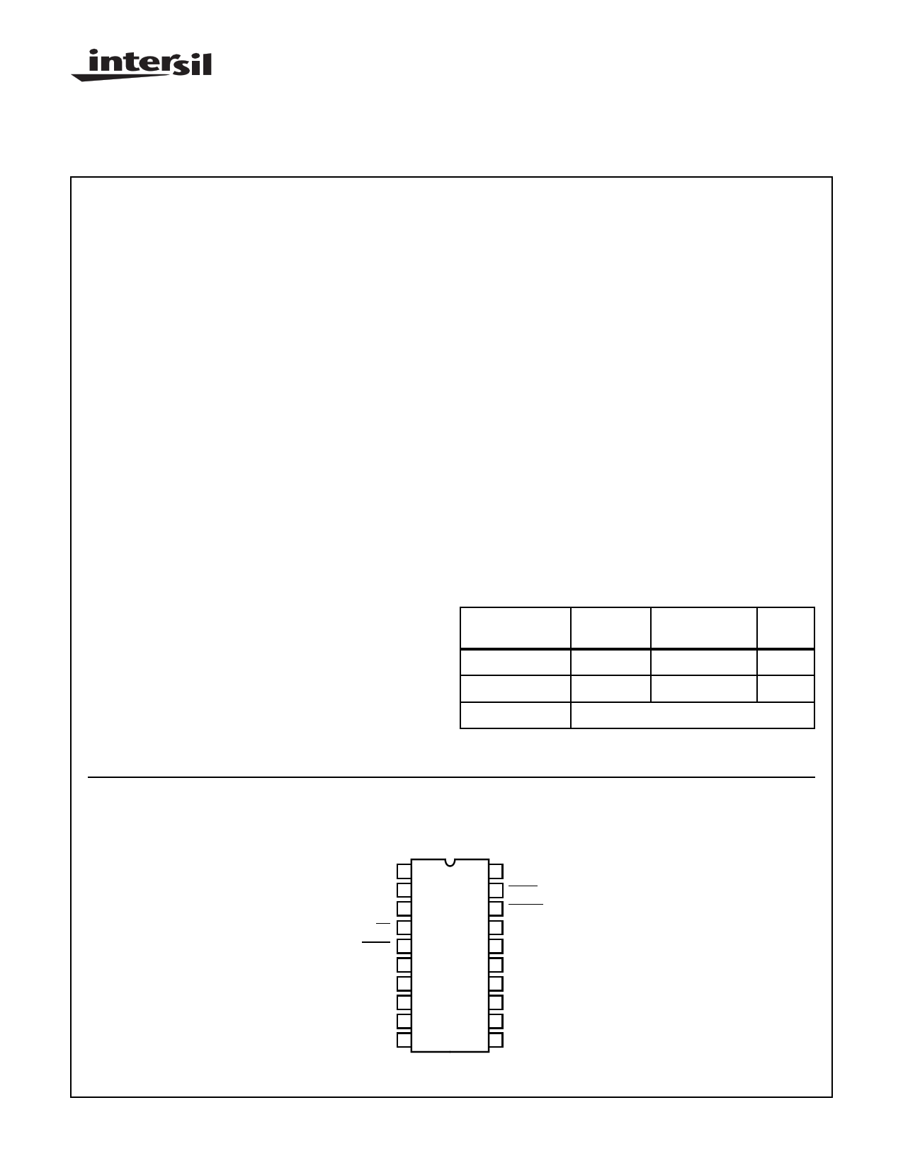
Pinout
HI7191
(PDIP, SOIC)
TOP VIEW
SCLK 1
SDO 2
SDIO 3
CS 4
DRDY 5
DGND 6
AVSS 7
VRLO 8
VRHI 9
VCM 10
20 MODE
19 SYNC
18 RESET
17 OSC1
16 OSC2
15 DVDD
14 AGND
13 AVDD
12 VINHI
11 VINLO
CAUTION: These devices are sensitive to electrostatic discharge; follow proper IC Handling Procedures.
http://www.intersil.com or 407-727-9207 | Copyright © Intersil Corporation 1999
1897
File Number 4138.3
1 page 
Timing Diagrams
CS
SCLK
tPRE
tDSU
HI7191
tSCLK
tSCLKPW
tSCLKPW
SDIO
1ST BIT
tDHLD
2ND BIT
FIGURE 1. DATA WRITE TO HI7191
CS
SCLK
SDIO
SDO
DRDY
CS
SCLK
SDIO
tACC
1ST BIT
tDV
FIGURE 2. DATA READ FROM HI7191
2ND BIT
tDRDY
15
67
FIGURE 3. DATA READ FROM HI7191
1901
8
5 Page 
HI7191
LOAD CELL
HI7191
AVDD
RATIOMETRIC
CONFIGURATION
CURRENT
SOURCE
VRHI
VRLO
VINHI
VINLO
AVSS
FIGURE 7. BURN-OUT CURRENT SOURCE CIRCUIT
Digital Section Description
A block diagram of the digital section of the HI7191 is shown
in Figure 9. This section includes a low pass decimation fil-
ter, conversion controller, calibration logic, serial interface,
and clock generator.
MODULATOR
CLOCK
CLOCK
GENERATOR
OSC2
OSC1
DIGITAL
FILTER
CALIBRATION
AND CONTROL
SERIAL I/O
SDO
SDIO
SCLK
CS
DRDY
SYNC
RESET
FIGURE 8. DIGITAL SECTION BLOCK DIAGRAM
Digital Filtering
One advantage of digital filtering is that it occurs after the
conversion process and can remove noise introduced during
the conversion. It can not, however, remove noise present on
the analog signal prior to the ADC (which an analog filter
can).
One problem with the modulator/digital filter combination is
that excursions outside the full scale range of the device
could cause the modulator and digital filter to saturate. This
device has headroom built in to the modulator and digital fil-
ter which tolerates signal deviations up to 33% outside of the
full scale range of the device. If noise spikes can drive the
input signal outside of this extended range, it is recom-
mended that an input analog filter is used or the overall input
signal level is reduced.
Low Pass Decimation Filter
The digital low-pass filter is a Hogenauer (sinc3) decimating
filter. This filter was chosen because it is a cost effective low
pass decimating filter that minimizes the need for internal
multipliers and extensive storage and is most effective when
used with high sampling or oversampling rates. Figure 10
shows the frequency characteristics of the filter where fC is
the -3dB frequency of the input signal and fN is the
programmed notch frequency. The analog modulator sends
a one bit data stream to the filter at a rate of that is
determined by:
fMODULATOR = fOSC/128
fMODULATOR = 78.125kHz for fOSC = 10MHz.
The filter then converts the serial modulator data into 40-bit
words for processing by the Hogenauer filter. The data is
decimated in the filter at a rate determined by the CODE
word FP10-FP0 (programed by the user into the Control
Register) and the external clock rate. The equation is:
fNOTCH = fOSC/(512 x CODE).
The Control Register has 11 bits that select the filter cutoff
frequency and the first notch of the filter. The output data
update rate is equal to the notch frequency. The notch fre-
quency sets the Nyquist sampling rate of the device while
the -3dB point of the filter determines the frequency spec-
trum of interest (fS). The FP bits have a usable range of 10
through 2047 where 10 yields a 1.953kHz Nyquist rate.
The Hogenauer filter contains alias components that reflect
around the notch frequency. If the spectrum of the frequency
of interest reaches the alias component, the data has been
aliased and therefore undersampled.
Filter Characteristics
Please note: We have recently discovered a performance
anomaly with the HI7191. The problem occurs when the
digital code for the notch filter is programmed within
certain frequencies. We believe the error is caused by
the calibration logic and the digital notch code NOT the
absolute frequency. The error is seen when the user
applies mid-scale (0V input, Bipolar mode). With this
input, the expected digital output should be mid-scale
(800000h). Instead, there is a small probability, of an
erroneous negative full scale (000000h)output. Refer to
Technical Brief TB348 for complete details.
The FP10 to FP0 bits programmed into the Control Register
determine the cutoff (or notch) frequency of the digital filter.
The allowable code range is 00AH. This corresponds to a
maximum and minimum cutoff frequency of 1.953kHz and
10Hz, respectively when operating at a clock frequency of
10MHz. If a 1MHz clock is used then the maximum and min-
imum cutoff frequencies become 195.3kHz and 1Hz, respec-
tively. A plot of the (sinx/x)3 digital filter characteristics is
shown in Figure 10. This filter provides greater than 120dB
of 50Hz or 60Hz rejection. Changing the clock frequency or
the programming of the FP bits does not change the shape
of the filter characteristics, it merely shifts the notch fre-
quency. This low pass digital filter at the output of the con-
1907
11 Page | ||
| Páginas | Total 24 Páginas | |
| PDF Descargar | [ Datasheet HI7191.PDF ] | |
Hoja de datos destacado
| Número de pieza | Descripción | Fabricantes |
| HI7190 | Sigma Delta A/D Converter | Intersil Corporation |
| HI7191 | Sigma Delta A/D Converter | Intersil Corporation |
| Número de pieza | Descripción | Fabricantes |
| SLA6805M | High Voltage 3 phase Motor Driver IC. |
Sanken |
| SDC1742 | 12- and 14-Bit Hybrid Synchro / Resolver-to-Digital Converters. |
Analog Devices |
|
DataSheet.es es una pagina web que funciona como un repositorio de manuales o hoja de datos de muchos de los productos más populares, |
| DataSheet.es | 2020 | Privacy Policy | Contacto | Buscar |