|
|
|
PDF HI3086 Data sheet ( Hoja de datos )
| Número de pieza | HI3086 | |
| Descripción | Flash A/D Converter | |
| Fabricantes | Intersil Corporation | |
| Logotipo | ||
Hay una vista previa y un enlace de descarga de HI3086 (archivo pdf) en la parte inferior de esta página. Total 18 Páginas | ||
|
No Preview Available !
August 2000
HI3086F®Oc1o-R8n8At8a-cPItNOOoTSBuESSrRIOTBSLeLIcLEEhToSnErUicwPBaRwlSOSwTuDI.TipnUUptCeTorTErstiPlC.RceoOn6mtDe-/UBrtsCacitTt, 140 MSPS, Flash A/D Converter
Features
• Differential Linearity Error. . . . . . . . . . . . . . . . . ±0.2 LSB
• Integral Linearity Error . . . . . . . . . . . . . . . . . . ±0.2 LSB
• Single +5V Power Supply Operation Available
• Low Input Capacitance . . . . . . . . . . . . . . . . . . . . . . . 7pF
• Wide Analog Input Bandwidth . . . . . . . . . . . . . 200MHz
• Low Power Consumption . . . . . . . . . . . . . . . . . . 360mW
• CLK/2 Clock Output Pin
• Excellent Temperature Characteristics
• 1:2 Demultiplexed Output
• Internal 1/2 Frequency Divider Circuit
(With Reset Function)
• Compatible with ECL, PECL and TTL Digital Input Levels
• Direct Replacement for Sony CXA3086
Applications
• RGB Graphics Processing (LCD, PDP)
www.DataSheet4U.com • Digital Communications (QPSK, QAM)
• Magnetic Recording (PRML)
Description
The HI3086 is a 6-bit, high-speed, flash analog-to-digital con-
verter optimized for high speed, low power, and ease of use.
With a 140 MSPS encode rate capability and full-power analog
bandwidth of 200MHz, this component is ideal for applications
requiring the highest possible dynamic performance.
To minimize system cost and power dissipation, only a +5V
power supply is required. The HI3086’s clock input interfaces
directly to TTL, ECL, or PECL logic and will operate with single-
ended inputs. The user may select 16-bit demultiplexed output
or 8-bit single-channel digital outputs. The demultiplexed mode
interleaves the data through two 8-bit channels at 1/2 the clock
rate. Operation in demultiplexed mode reduces the speed and
cost of external digital interfaces, while allowing the A/D
converter to be clocked to the full 140 MSPS conversion rate.
Fabricated with an advanced bipolar process, the HI3086 is
provided in a space-saving 48-lead MQFP surface mount
plastic package and is specified over the -20oC to 75oC
temperature range.
Part Number Information
PART
NUMBER
HI3086JCQ
HI3086EVAL
TEMP.
RANGE (oC) PACKAGE
PKG. NO.
-20 to 75 48 Ld MQFP Q48.12x12-S
25 Evaluation Board
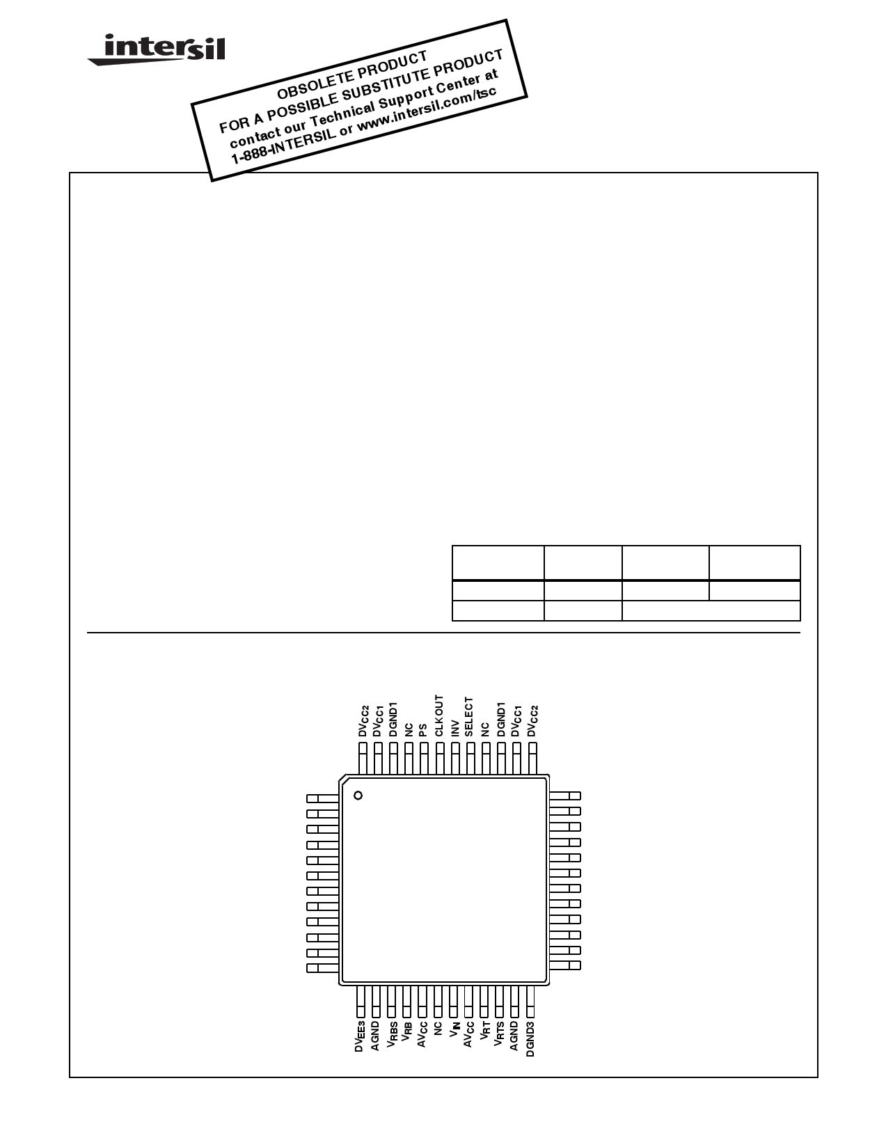
Pinout
HI3086 (MQFP)
TOP VIEW
DGND2
P2D0 (LSB)
P2D1
P2D2
P2D3
P2D4
P2D5 (MSB)
DGND2
DVCC2
RESETN/T
RESET/E
RESETN/E
48 47 46 45 44 43 42 41 40 39 38 37
1 36
2 35
3 34
4 33
5 32
6 31
7 30
8 29
9 28
10 27
11 26
1213
14
15
16
17
18
19
20
21 22
25
23 24
DGND2
P1D5 (MSB)
P1D4
P1D3
P1D2
P1D1
P1D0 (LSB)
DGND2
DVCC2
CLK/T
CLKN/E
CLK/E
CCAUTION: These devices are sensitive to electrostatic discharge; follow proper IC Handling Procedures.
1-888-INTERSIL or 321-724-7143 | Intersil (and design) is a registered trademark of Intersil Americas Inc.
Copyright © Intersil Americas Inc. 2002. All Rights Reserved
1
File Number 4110.2
1 page 
Pin Descriptions (Continued)
PIN
NO.
SYMBOL
I/O
TYPICAL
VOLTAGE
LEVEL
22
VRTS
O +4.0V (Typ)
21 VRT I VRTS + R1 x IREF
16 VRB I VRBS -R2 x IREF
15
VRBS
O +2.0V (Typ)
HI3086
EQUIVALENT CIRCUIT
22
R1
21
R
R
R
R
COMPARATOR 1
COMPARATOR 2
R
R
R
R2
16
R
15
COMPARATOR 62
COMPARATOR 63
DESCRIPTION
Reference Voltage Sense. Bypass
to AGND with a 0.1µF chip
capacitor.
Top Reference Voltage. Bypass to
AGND with a 1µF tantal capacitor
and 0.1µF chip capacitor.
Bottom Reference Voltage. Bypass
to AGND with a 1µF tantal capacitor
and a 0.1µF chip capacitor.
Reference Voltage Sense. Bypass
to AGND with a 0.1µF chip
capacitor.
19 VIN I VRT to VRB
COMPARATOR
AVCC
AVCC
Analog Input.
30 to 35 P1D0 to P1D5 O TTL
2 to 7 P2D0 to P2D5 O
43
CLKOUT
O
19
DVEE3
DVCC1
AGND
DGND1
VREF
DVCC2
Port 1 Side Data Output.
Port 2 Side Data Output.
2 TO 7
30 TO 35
43
DGND2
DVEE3
Clock Output. (See Table 2.
Operating Mode Table.)
5
5 Page 
HI3086
CLK
CLK
HI3086
CLK A
RESETN
6-BITS
CLKOUT
DATA
HI3086
CLK B
RESETN
6-BITS
CLKOUT
DATA
FIGURE 8. WHEN THE RESET PULSE IS NOT USED
CLK
RESET PULSE
HI3086
CLK A
RESETN
6-BITS
CLK
RESET
PULSE
CLKOUT
DATA
HI3086
CLK B
RESETN
6-BITS
CLKOUT
DATA
FIGURE 9. WHEN THE RESET PULSE IS USED
Straight Mode (See Figures 22, 23, 24 and 25).
Set the SELECT pin to GND for this mode. In this mode,
data output can be obtained in accordance with the clock fre-
quency applied to the A/D converter for applications which
use the clock applied to the A/D converter as the system
clock.
The A/D converter can operate at fC (Min) = 100 MSPS in
this mode.
Digital Input Level and Supply Voltage Settings
The logic input level for the HI3086 supports ECL, PECL and
TTL levels. The power supplies (DVEE3, DGND3) for the
logic input block must be set to match the logic input (CLK
and RESET signals) level.
TABLE 3. LOGIC INPUT LEVEL AND POWER SUPPLY SETTINGS
DIGITAL
INPUT
LEVEL
ECL
DVEE3
-5V
PECL
0V
DGND3
0V
+5V
SUPPLY APPLICATION
VOLTAGE CIRCUITS
±5V Figures 19, 22
+5V Figures 20, 23
TTL 0V +5V
+5V Figures 21, 24, 25
11
11 Page | ||
| Páginas | Total 18 Páginas | |
| PDF Descargar | [ Datasheet HI3086.PDF ] | |
Hoja de datos destacado
| Número de pieza | Descripción | Fabricantes |
| HI3086 | Flash A/D Converter | Intersil Corporation |
| Número de pieza | Descripción | Fabricantes |
| SLA6805M | High Voltage 3 phase Motor Driver IC. |
Sanken |
| SDC1742 | 12- and 14-Bit Hybrid Synchro / Resolver-to-Digital Converters. |
Analog Devices |
|
DataSheet.es es una pagina web que funciona como un repositorio de manuales o hoja de datos de muchos de los productos más populares, |
| DataSheet.es | 2020 | Privacy Policy | Contacto | Buscar |