|
|
|
PDF HI5905QML Data sheet ( Hoja de datos )
| Número de pieza | HI5905QML | |
| Descripción | A/D Converter | |
| Fabricantes | Intersil Corporation | |
| Logotipo | ||
Hay una vista previa y un enlace de descarga de HI5905QML (archivo pdf) en la parte inferior de esta página. Total 8 Páginas | ||
|
No Preview Available !
TM
Data Sheet
HI5905N/QML
July 1999 File Number 4718.1
14-Bit, 5 MSPS, Military A/D Converter
The HI5905N/QML is a monolithic, 14-bit, 5MSPS Analog-
to-Digital Converter fabricated in an advanced BiCMOS
process. It is designed for high speed, high resolution
applications where wide bandwidth, low power consumption
and excellent SINAD performance are essential. With a
100MHz full power input bandwidth and high frequency
accuracy, the converter is ideal for many Military types of
communication systems employing digital IF architectures.
The HI5905N/QML is designed in a fully differential pipelined
architecture with a front end differential-in-differential-out
sample-and-hold amplifier (S/H). Consuming 350mW (typ)
power at 5MSPS, the HI5905N/QML has excellent dynamic
performance over the full Military temperature range.
Data output latches are provided which present valid data to
the output bus with a data latency of only 4 clock cycles.
Specifications for QML devices are controlled by the
Defense Supply Center in Columbus (DSCC). The SMD
numbers listed below must be used when ordering.
Detailed Electrical Specifications for the HI5905N/QML
are contained in SMD 5962-98591. That document may
be easily downloaded from our website.
http://www.Intersil.com/data/sm/index.htm
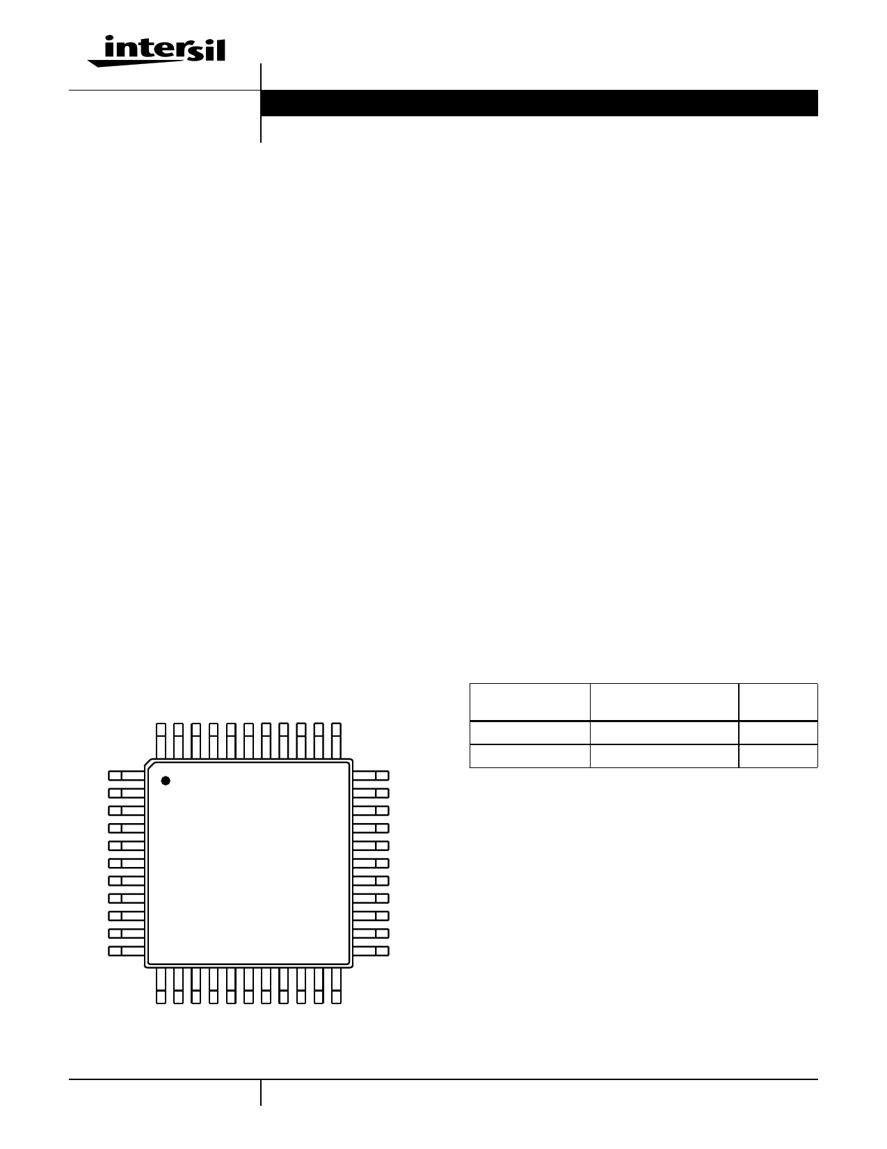
Pinout
HI5905 (MQFP) (MO-108AA-2 ISSUE A)
TOP VIEW
NC
NC
DGND1
NC
AVCC
AGND
NC
NC
VIN+
VIN-
VDC
44 43 42 41 40 39 38 37 36 35 34
1 33
2 32
3 31
4 30
5 29
6 28
7 27
8 26
9 25
10 24
11 23
12 13 14 15 16 17 18 19 20 21 22
D3
D4
D5
D6
D7
NC
DVCC2
DGND2
D8
D9
NC
Features
• QML Compliant per SMD 5962-9859101NXB
• Sampling Rate . . . . . . . . . . . . . . . . . . . . . . . . . . . .5MSPS
• Low Power at 5MSPS. . . . . . . . . . . . . . . . . 400mW (Max)
• Internal Sample and Hold
• Fully Differential Architecture
• Full Power Input Bandwidth . . . . . . . . . . . . . . . . . 100MHz
• SINAD at 1MHz . . . . . . . . . . . . . . . . . . . . . . >69dB (Min)
• Internal Voltage Reference
• TTL Compatible Clock Input
• CMOS Compatible Digital Data Outputs
Applications
• Digital Communication Systems
• Undersampling Digital IF
• Asymmetric Digital Subscriber Line (ADSL)
• Document Scanners
• Reference Literature
- AN9214, Using Intersil High Speed A/D Converters
- AN9785, Using the Intersil HI5905 EVAL2 Evaluation
Board
Ordering Information
ORDERING
NUMBER
INTERNAL INTERSIL
MKT. NUMBER
5962-9859101NXB HI5905N/QML
HI5905EVAL2
Low Frequency Platform
TEMP.
RANGE(oC)
-55 to 125
25
4-1 CAUTION: These devices are sensitive to electrostatic discharge; follow proper IC Handling Procedures.
1-888-724-7143 | Copyright © Intersil Corporation 1999
1 page 
identical four-bit subconverter stages with the corresponding
output of the fifth stage flash converter before applying the
twenty bit result to the digital error correction logic. The
digital error correction logic uses the supplementary bits to
correct any error that may exist before generating the final
fourteen bit digital data output of the converter.
Because of the pipeline nature of this converter, the digital
data representing an analog input sample is output to the
digital data bus on the 4th cycle of the clock after the analog
sample is taken. This time delay is specified as the data
latency. After the data latency time, the digital data
representing each succeeding analog sample is output
during the following clock cycle. The digital output data is
synchronized to the external sampling clock with a latch. The
digital output data is available in two’s complement binary
format (see Table 1, A/D Code Table).
Internal Reference Generator, VROUT and VRIN
The HI5905 has an internal reference generator, therefore, no
external reference voltage is required. VROUT must be
connected to VRIN when using the internal reference voltage.
The HI5905 can be used with an external reference. The
converter requires only one external reference voltage
connected to the VRIN pin with VROUT left open.
The HI5905 is tested with VROUT, equal to 4.0V, connected
to VRIN. Internal to the converter, two reference voltages of
1.3V and 3.3V are generated for a fully differential input
signal range of ±2V.
In order to minimize overall converter noise, it is
recommended that adequate high frequency decoupling be
provided at the reference voltage input pin, VRIN.
Analog Input, Differential Connection
The analog input to the HI5905 can be configured in various
ways depending on the signal source and the required level
of performance. A fully differential connection (Figure 4) will
give the best performance for the converter.
Since the HI5905 is powered off a single +5V supply, the
analog input must be biased so it lies within the analog input
common mode voltage range of 1.0V to 4.0V. The
performance of the ADC does not change significantly with
the value of the analog input common mode voltage.
VIN VIN+
HI5905
VDC
-VIN
VIN-
FIGURE 4. AC COUPLED DIFFERENTIAL INPUT
A 2.3V DC bias voltage source, VDC, half way between the
top and bottom internal reference voltages, is made
available to the user to help simplify circuit design when
using a differential input. This low output impedance voltage
source is not designed to be a reference but makes an
excellent bias source and stays within the analog input
common mode voltage range over temperature.
The difference between the converter’s two internal voltage
references is 2V. For the AC coupled differential input, (Figure
4), if VIN is a 2VP-P sinewave with -VIN being 180 degrees out of
phase with VIN, then VIN+ is a 2VP-P sinewave riding on a DC
bias voltage equal to VDC and VIN- is a 2VP-P sinewave riding
on a DC bias voltage equal to VDC. Consequently, the converter
will be at positive full scale, resulting in a digital data output code
with D13 (MSB) equal to a logic “0” and D0-D12 equal to logic
“1” (see Table 1, A/D Code Table), when the VIN+ input is at
VDC+1V and the VIN- input is at VDC-1V (VIN+ - VIN- = 2V).
Conversely, the ADC will be at negative full scale, resulting in a
digital data output code with D13 (MSB) equal to a logic “1” and
D0-D12 equal to logic “0” (see Table 1, A/D Code Table), when
the VIN+ input is equal to VDC-1V and VIN- is at VDC+1V
(VIN+-VIN- = -2V). From this, the converter is seen to have a
peak-to-peak differential analog input voltage range of 2V.
The analog input can be DC coupled (Figure 5) as long as
the inputs are within the analog input common mode voltage
range (1.0V ≤ VDC ≤ 4.0V).
TABLE 1. A/D CODE TABLE
DIFFERENTIAL
TWO’S COMPLEMENT BINARY OUTPUT CODE
CODE
CENTER
INPUT VOLTAGE † MSB
(USING INTERNAL
LSB
DESCRIPTION REFERENCE) D13 D12 D11 D10 D9 D8 D7 D6 D5 D4 D3 D2 D1 D0
+Full Scale
+1.99994V
(+FS) - 1/4 LSB
+FS - 1 1/4 LSB 1.99969V
01111111111111
01111111111110
+ 3/4 LSB
- 1/4 LSB
183.105µV
-61.035µV
00000000000000
11111111111111
-FS + 1 3/4 LSB -1.99957V
10000000000001
-Full Scale
-1.99982V
(-FS) + 3/4 LSB
10000000000000
† The voltages listed above represent the ideal center of each two’s complement binary output code shown.
4-5
5 Page | ||
| Páginas | Total 8 Páginas | |
| PDF Descargar | [ Datasheet HI5905QML.PDF ] | |
Hoja de datos destacado
| Número de pieza | Descripción | Fabricantes |
| HI5905QML | A/D Converter | Intersil Corporation |
| Número de pieza | Descripción | Fabricantes |
| SLA6805M | High Voltage 3 phase Motor Driver IC. |
Sanken |
| SDC1742 | 12- and 14-Bit Hybrid Synchro / Resolver-to-Digital Converters. |
Analog Devices |
|
DataSheet.es es una pagina web que funciona como un repositorio de manuales o hoja de datos de muchos de los productos más populares, |
| DataSheet.es | 2020 | Privacy Policy | Contacto | Buscar |