|
|
PDF HD49335HF Data sheet ( Hoja de datos )
| Número de pieza | HD49335HF | |
| Descripción | CDS/PGA AND 10-bit A/D TG Converter | |
| Fabricantes | Renesas Technology | |
| Logotipo |  |
|
Hay una vista previa y un enlace de descarga de HD49335HF (archivo pdf) en la parte inferior de esta página. Total 30 Páginas | ||
|
No Preview Available !
www.DataSheet4U.com
HD49335F/HF
CDS/PGA & 10-bit A/D TG Converter
REJ03F0100-0100Z
Rev.1.0
Feb.25.2004
Description
The HD49335F/HF is a CMOS IC that provides CDS-PGA analog processing (CDS/PGA) suitable for CCD camera
digital signal processing systems together with a 10-bit A/D converter and timing generator in a single chip.
There are address map and timing generator charts besides this specification. May be contacted to our sales department
if examining the details.
Functions
• Correlated double sampling
• PGA
• Serial interface control
• 10-bit ADC
• Timing generator
• Operates using only the 3 V voltage
• Corresponds to switching mode of power dissipation and operating frequency
Power dissipation: 220 mW (Typ), maximum frequency: 36 MHz (HD49335HF)
Power dissipation: 150 mW (Typ), maximum frequency: 25 MHz (HD49335F)
• ADC direct input mode
• QFP 64-pin package
Features
• Suppresses low-frequency noise, which output from CCD by the correlated double sampling.
• The S/H response frequency characteristics for the reference level can be adjusted using values of external parts and
registers.
• High sensitivity is achieved due to the high S/N ratio and a wide dynamic range provided by a PG amplifier.
• PGA, pulse timing, standby mode, etc., is achieved via a serial interface.
• High precision is provided by a 10-bit-resolution A/D converter.
• Difference encoded gray code can be selected as an A/D output code. It is effective in suppression of solarization
(wave pattern). It is patented by Renesas.
• Timing generator generates the all of pulse which are needed for CCD driving.
Rev.1.0, Feb.25.2004, page 1 of 29
1 page 
HD49335F/HF
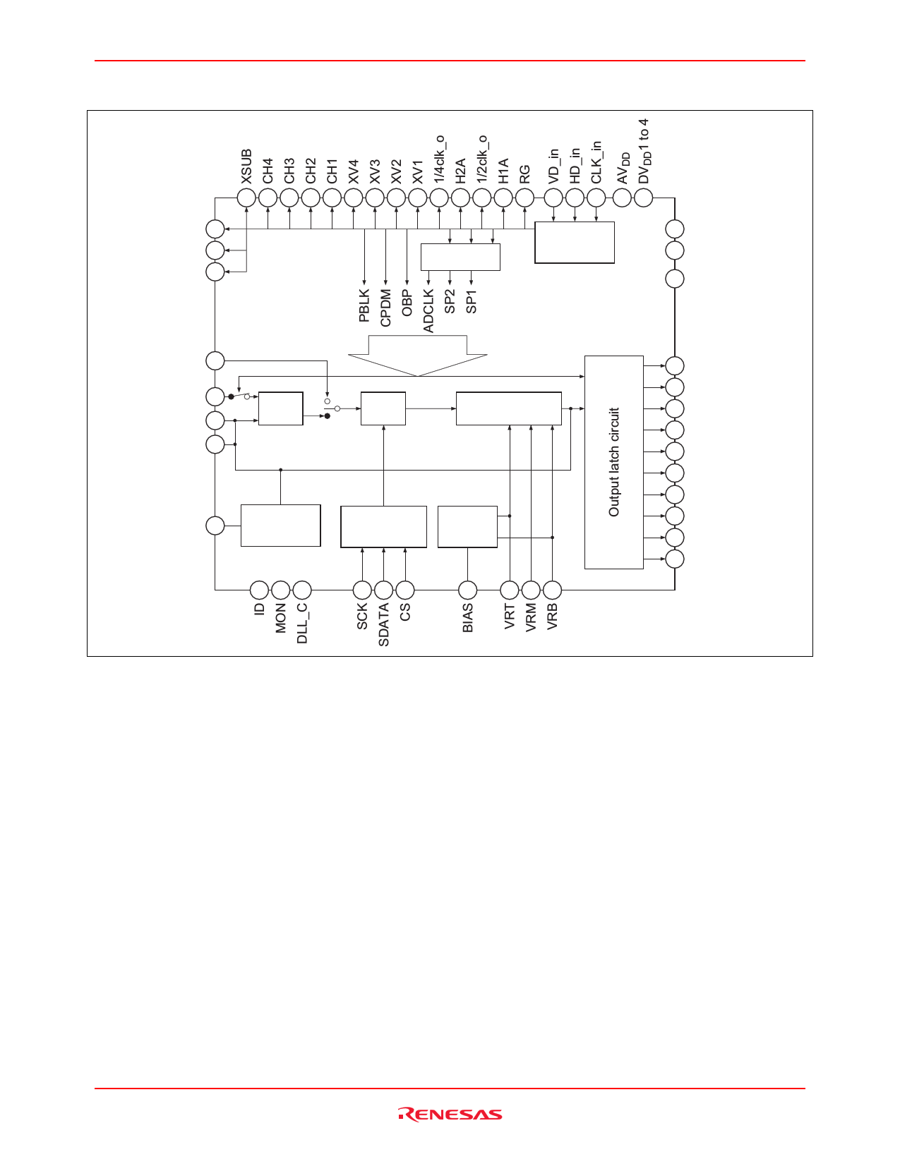
Block Diagram
SUB_SW
SUB_PD
STROB
Timing
DLL generator
ADC_in
CDS_in
BLKSH
BLKC
CDS
PGA
10bit
ADC
BLKFB
DC offset
compensation
circuit
Serial
interface
Bias
generator
AVSS
DVSS1 to 4
Reset
D9
D8
D7
D6
D5
D4
D3
D2
D1
D0
Rev.1.0, Feb.25.2004, page 5 of 29
5 Page 
HD49335F/HF
Detailed Timing Specifications
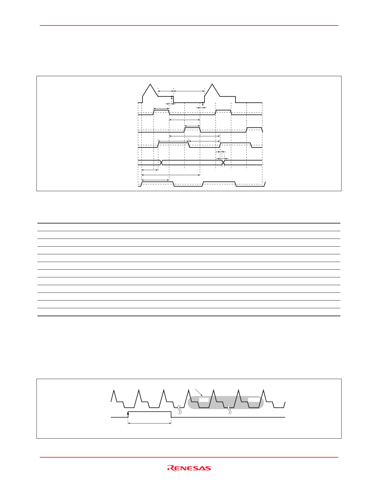
Detailed Timing Specifications when CDSIN Input Mode is Used
Figure 3 shows the detailed timing specifications when the CDSIN input mode is used, and table 8 shows each timing
specification.
CDS_in
SP1
SP2
ADCLK
D0 to D9
H1
Black
level
Signal
level
(2) (1)
(3)
(5)
(4)
(6)
(7) (8)
(11)
(13)
(12)
(9)
(10)
Vth
Vth
Vth
Figure 3 Detailed Timing Chart when CDSIN Input Mode is Used
Table 8 Timing Specifications when the CDSIN Input Mode is Used
No.
(1)
(2)
(3)
(4)
(5)
(6)
(7), (8)
(9)
(10)
(11)
(12)
(13)
Timing
Black-level signal fetch time
SP1 ‘Hi’ period
Signal-level fetch time
SP2 ‘Hi’ period
SP1 falling to SP2 falling time
SP1 falling to ADCLK rising inhibit time
ADCLK tWH min./tWL min
ADCLK rising to digital output holding time
ADCLK rising to digital output delay time
H1 rising to ADCLK rising time
H1 rising to SPSIG falling time
H1 rising to SPBLK falling time
Symbol
tCDS1
tCDS2
tCDS3
tCDS4
tCDS5
tCDS6
tCDS7, 8
tCHLD9
tCOD10
tCDS11
tCDS12
tCDS13
Min
—
Typ × 0.8
—
Typ × 0.8
Typ × 0.85
—
11
—
—
—
—
—
Typ
(1.5)
1/4fCLK
(1.5)
1/4fCLK
1/2fCLK
(5)
—
(7)
(16)
(1/4fCLK)
(1/fCLK)
(1/2fCLK)
Max
—
Typ × 1.2
—
Typ × 1.2
Typ × 1.15
—
—
—
—
—
—
—
Unit
ns
ns
ns
ns
ns
ns
ns
ns
ns
ns
ns
ns
OBP Detailed Timing Specifications
Figure 4 shows the OBP detailed timing specifications.
The OB period is from the fifth to the twelfth clock cycle after the OB pulse is inputted. The average of the black
signal level is taken for eight input cycles during the OB period and it becomes the clamp level (DC standard).
OB period *1
CDS_in N N+1
N+5 N+12
OBP
OB pulse > 2 clock cycles
Note: 1. Shifts ±1 clock cycle depending on the OBP input timing.
Figure 4 OBP Detailed Timing Specifications
N+13
Rev.1.0, Feb.25.2004, page 11 of 29
11 Page | ||
| Páginas | Total 30 Páginas | |
| PDF Descargar | [ Datasheet HD49335HF.PDF ] | |
Hoja de datos destacado
| Número de pieza | Descripción | Fabricantes |
| HD49335HF | CDS/PGA AND 10-bit A/D TG Converter | Renesas Technology |
| HD49335HNP | CDS/PGA & 10-bit A/D TG Converter | Renesas Technology |
| Número de pieza | Descripción | Fabricantes |
| SLA6805M | High Voltage 3 phase Motor Driver IC. |
Sanken |
| SDC1742 | 12- and 14-Bit Hybrid Synchro / Resolver-to-Digital Converters. |
Analog Devices |
|
DataSheet.es es una pagina web que funciona como un repositorio de manuales o hoja de datos de muchos de los productos más populares, |
| DataSheet.es | 2020 | Privacy Policy | Contacto | Buscar |
