|
|
|
PDF 82C283 Data sheet ( Hoja de datos )
| Número de pieza | 82C283 | |
| Descripción | 386SX System Controller | |
| Fabricantes | Opti | |
| Logotipo | ||
Hay una vista previa y un enlace de descarga de 82C283 (archivo pdf) en la parte inferior de esta página. Total 24 Páginas | ||
|
No Preview Available !
OPTiwww.DataSheet4U.com
®
1.0 Features
• Flexible DRAM banks configuration
- Supports 256K, 1M and 4M DRAM
• Block interleave mode operations
- Block interleaving at a block size of 512 bytes
• BIOS shadow RAM
- Shadow RAM for system, video and adapter BIOS
• Memory remapping
• Flexible multiplexed DRAM address
• Programmable AT bus clock
• Turbo switch
• 160-pin PQFP (Plastic Quad Flat Pack)
82C283
386SX System Controller
2.0 Overview
The 82C283 is a highly integrated, AT system logic VLSI chip
for high-end 386SX/AT systems. It integrates a local memory
controller (local memory is on-board memory), AT bus con-
troller, and data bus controller into one chip. It is designed for
systems running at 16MHz, 20MHz, 25MHz, and 33MHz*. A
high performance, compact 386SX/AT system is readily
implemented with the 82C283 and a standard peripheral con-
troller like OPTi’s 82C206 or the 82C100 (with Dallas Semi-
conductor (DS1287).
*Rev. B only
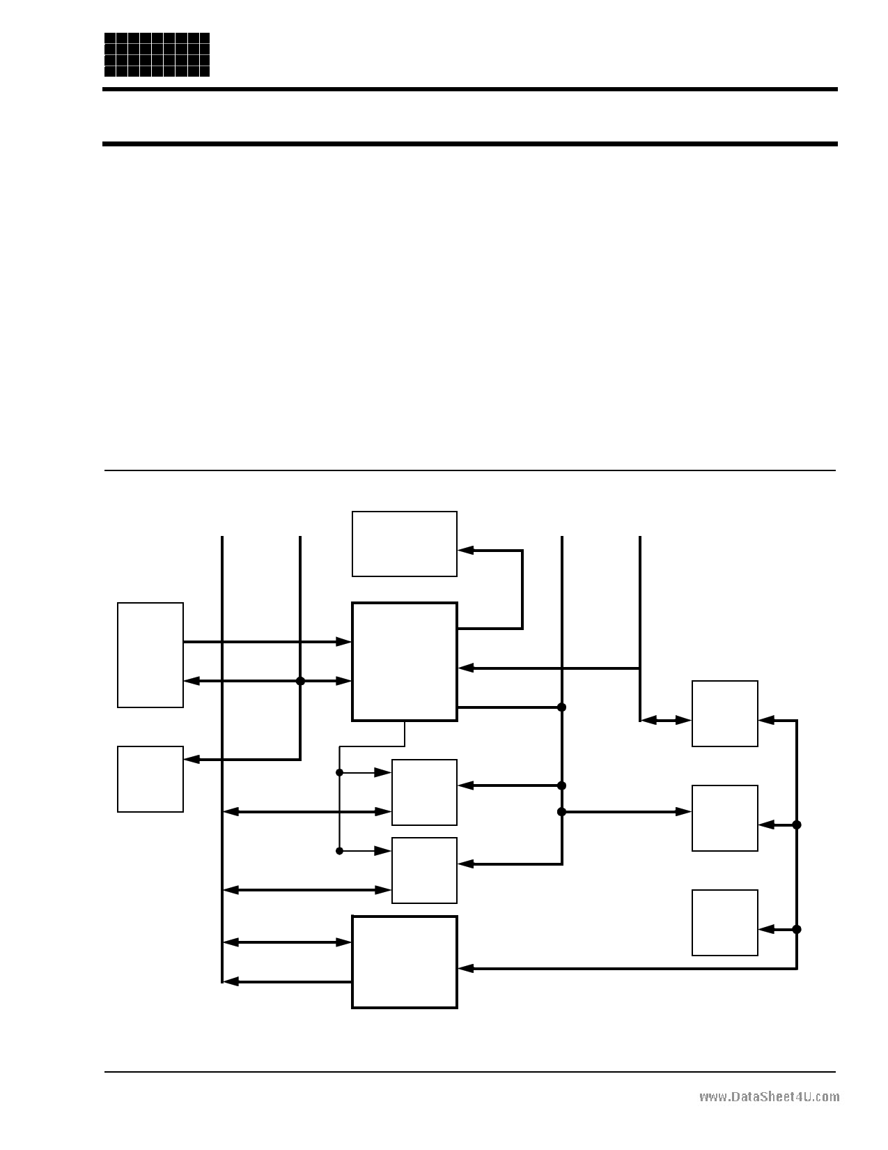
Figure 2-1 System Block Diagram
A Bus
D Bus
DRAM
RAS, CAS, SA Bus
MA
SD Bus
386SX
387SX
A[23:0]
D[15:0]
D[15:0]
XA0
A[16:1]
GA20
A[23:17]
A[9:1]
A[23:16]
OPTi
82C283
245
(x2)
245
OPTi
82C206
SD[15:0]
SA[19:17]
SA[16:0]
LA[23:17]
XD[7:0]
SD 245
XD[7:0]
SA
ROM
8042
September 1994
OPTi Inc. · 2525 Walsh Avenue · Santa Clara, CA 95051 · (408) 980-8178
1 page 
www.DataSheet4U.com
82C283
3.1 Signal Descriptions
3.1.1 Clock and Reset Interface Signals
Signal Name
Pin No.
Signal
Type Signal Description
CLKI
PCLK2
OSC12
OSC
43 I CLK2 input from oscillator.
22 I/O CLK2 output to 386SX and 387SX. (Bidirectional output is always enabled.)
104 O 1.19MHz output.
18 I 14.31818MHz oscillator input.
3.1.2 CPU Control and Interface Signals
Signal Name
Pin No.
Signal
Type Signal Description
A[23:17]
67:61
I CPU Address Bus: Address lines 23 through 17 and 7 through 0.
A[16:8]
60:52
I/O CPU Address Bus: Address lines 16 through 8. These signals are inputs except
during DMA cycles. A[16:9] become outputs and convey DMA address 16-9 for
16-bit DMA cycles. A[15:8] become outputs and convey DMA address 15-8 for 8-
bit DMA cycles. A[10:9] are outputs during refresh.
A[7:0]
51:44
I/O CPU Address Bus: Address lines 7 through 0. These inputs become outputs dur-
ing refresh.
D[15:0]
MP[1:0]
9:2,
158:151
150, 149
I/O Data bus to/from the CPU.
I/O Local DRAM parity bits 1 and 0.
RDYI#
RDY#
32 I Ready input from coprocessor Ready.
16 O Ready output to the CPU to terminate the current cycle.
NA#
CPURST
33 O CPU next address control signal.
24 O CPU reset signal.
NMI
WR#
23 O Non-maskable interrupt.
15 I Write or Read is a bus cycle definition pin that distinguishes write cycles from
reads cycles.
DC#
MIO#
ADS#
14 I Data or Control is a bus cycle definition pin that distinguishes data cycles from
control cycles.
13 I Memory or I/O is a bus cycle definition pin that distinguishes memory cycles from
input/output cycles.
12 I Address status from the 386SX.
HOLD
11 O Hold request to the 386SX
HLDA
BHE#
10 I Hold acknowledge from the 286SX.
17 I/O Byte high enable from the CPU. It is an input during CPU cycles and an output
during non-CPU cycles.
912-3000-012
OPTi
®
Page 5
5 Page 
www.DataSheet4U.com
82C283
5.0 Configuration Registers
There are seven Configuration Registers inside the 82C283.
An indexing scheme is used to access all of these registers.
Port 22h is used as the Index Register and Port 24h is the
Data Register. Each access to a Configuration Register con-
sists of a write to Port 22h, specifying the desired register in
the data byte, followed by a read or write to Port 24h with the
actual register data. The index resets after every access;
therefore every data access (via Port 24h) must be preceded
by a write to Port 22h, even if the same register is being
accessed on consecutive occasions. All reserved bits are set
to zero by default.
Table 5-1 DRAM Configuration Register - Index 10h
Bit(s) Type Default
Function
7 RO 0 82C283 revision number:
0 = Revision A
1 = Revision B
6
R/W
0 Revision A:
Reserved - Must always = 0.
Revision B:
0 = Non-pipelined
1 = Pipelined
5
R/W
1 Local DRAM read cycle wait state:
0 = Zero wait state
1 = One wait state
4
R/W
1 Local DRAM write cycle wait state:
0 = Zero wait state
1 = One wait state
3:0 R/W 1111 Local DRAM memory configuration:
Bits
1111
0001
0010
0011
0100
0101
0110
0111
1000
1001
1010
1011
1100*
Bank 0 Bank 1 Bank 2 Bank 3 Total
256K 256K
1M
256K 256K 256K 256K 2M
256K 256K 1M
3M
256K 256K 1M 1M 5M
256K 256K 4M
9M
2M
1M 1M
4M
1M 1M 1M
6M
1M 1M 1M 1M 8M
1M 4M
10M
1M 1M 4M
12M
4M 4M
16M
4M 8M
*Rev. B Only
912-3000-012
OPTi
®
Page 11
11 Page | ||
| Páginas | Total 24 Páginas | |
| PDF Descargar | [ Datasheet 82C283.PDF ] | |
Hoja de datos destacado
| Número de pieza | Descripción | Fabricantes |
| 82C28 | VOLTAGE DETECTORS | Unisonic Technologies |
| 82C28 | VOLTAGE DETECTORS | Unisonic Technologies |
| 82C283 | 386SX System Controller | Opti |
| 82C284 | Clock Generator and Ready Interface for 80C286 Processors | Intersil Corporation |
| Número de pieza | Descripción | Fabricantes |
| SLA6805M | High Voltage 3 phase Motor Driver IC. |
Sanken |
| SDC1742 | 12- and 14-Bit Hybrid Synchro / Resolver-to-Digital Converters. |
Analog Devices |
|
DataSheet.es es una pagina web que funciona como un repositorio de manuales o hoja de datos de muchos de los productos más populares, |
| DataSheet.es | 2020 | Privacy Policy | Contacto | Buscar |