|
|
|
PDF SC4808B-2 Data sheet ( Hoja de datos )
| Número de pieza | SC4808B-2 | |
| Descripción | High Performance Dual Ended PWM Controller | |
| Fabricantes | Semtech Corporation | |
| Logotipo | ||
Hay una vista previa y un enlace de descarga de SC4808B-2 (archivo pdf) en la parte inferior de esta página. Total 28 Páginas | ||
|
No Preview Available !
POWER MANAGEMENT
Description
The SC4808B-2 is a dual-ended, high frequency, integrated
PWM controller, optimized for isolated applications that
require minimum space. It can be configured for current
or voltage mode operation with required control circuitry
where secondary side error amplifier is used.
Some of the key features are high frequency operation of
1 MHz that allows the use of smaller components thus
saving cost and valuable board space. An internal ramp
www.DataoShneett4hUe.coCmurrent Sense pin allows Internal Slope
Compensation programmed by an external resistor. Other
features include programmable frequency up to 1MHz,
Pulse by Pulse current and Line Monitoring Input with
Hysteresis to reduce stress on the power components.
A unique oscillator is used to synchronize two SC4808B-
2’s to work out of phase. This minimizes the input and
output ripple thus reducing noise on the output line and
reducing stress and size of input/output filter components.
The dual outputs can be configured in Push-Pull, Half Bridge
and Full Bridge format with programmable dead time
between two outputs depending on the size of the timing
components.
The SC4808B-2 also features a turn on threshold of 4.4V
and is available in MSOP-10 package.
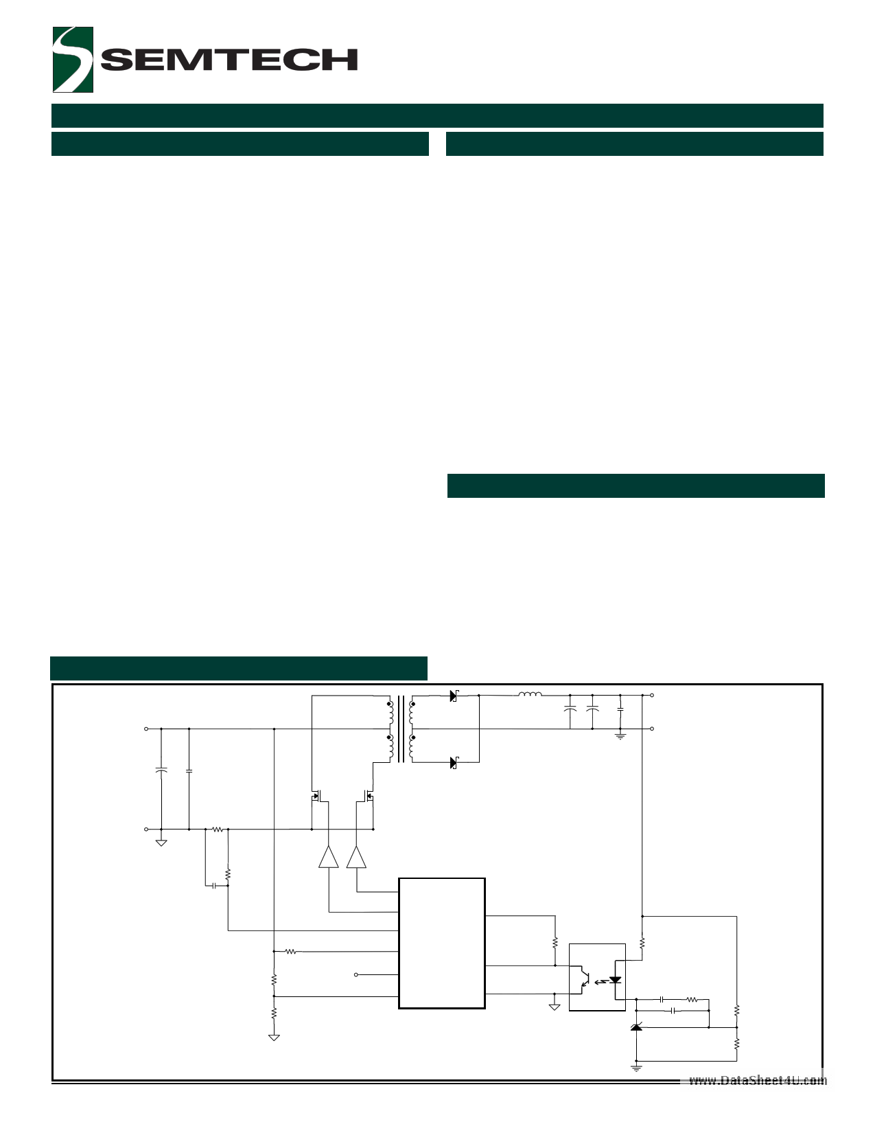
Typical Application Circuit
SC4808B-2
High Performance Dual
Ended PWM Controller
Features
120µA starting current
Pulse by pulse current limit
Programmable operation up to 1MHz
Internal soft start
Programmable line undervoltage lockout
Over current shutdown
Dual output drive stages on push-pull configuration
Programmable internal slope compensation
Programmable mode of operation (peak current mode
or voltage mode)
External frequency synchronization
Bi-phase mode of operation
-40 to 105 °C operating temperature
MSOP-10 Lead-free package. This product is fully WEEE
and RoHS compliant
Applications
Telecom equipment and power supplies
Networking power supplies
Industrial power supplies
Push-pull converter
Half bridge converter
Full bridge converter
Isolated VRM’s
Vo
Vin Gnd_Out
Gnd_In
RSENSE
Revision: May 3, 2006
OUTA RC
OUTB REF
CS
SYNC
VCC
SYNC
FB
LUVLO GND
SC4808
1
www.semtech.com
1 page 
SC4808B-2
POWER MANAGEMENT
Pin Descriptions
FB: The inverting input to the PWM comparator. Stray in-
ductances and parasitic capacitance should be minimized
by utilizing ground planes and correct layout guide lines
(see page 19).
REF: A 0.1µF or 47nF low ESR capacitor is required and
must be placed right at the pin.
CS: Current sense input and internal slope compensation
www.DataaSrheeebt4oUt.hcopmrovided via the CS pin. The current sense input
from a sense resistor is used for the peak current and
overcurrent comparators. An internal 1 to 3 feed back volt-
age divider provides a 3X amplification of the CS signal.
This is used for comparison to the external error amplifier
signal. If an external resistor is connected from CS to the
current sense resistor, the internal current source will pro-
vide a programmable slope compensation. The value of
the resistor will determine the level of compensation. At
higher compensation levels, voltage mode of operation can
be achieved.
RC: The oscillator programming pin. The oscillator should
be referenced to a stable reference voltage for an accu-
rate and stable frequency. Only two components are re-
quired to program the oscillator, a resistor (tied to Vref and
RC), and a capacitor (tied to the RC and GND). The follow-
ing formula can be used for a close approximation of the
oscillator frequency.
FOSC _ A
≅
1
ROSC CTOT
× 0.8
FOSC _ B
≅
1
ROSC CTOT
× 0.9
where:
CTOT = COSC + CSC 4808 + CCircuit
LUVLO: Line undervoltage lockout pin. An external resis-
tive divider will program the undervoltage lockout level. The
external divider should be referenced to the quiet analog
ground (see page 19). During the LUVLO, the driver out-
puts are disabled and the softstart is reset. This pin can
also function as an Enable/Disable.
SYNC: SYNC is a positive edge triggered input with a thresh-
old set to 1.0V. In a single controller operation, SYNC could
be grounded or connected to an external synchronization
clock within the SYNC frequency range (see page 3). In
the Bi-Phase operation mode SYNC pins could be con-
nected to the Cosc (Timing Capacitors) of the other con-
troller. This will force an out of phase operation (see page
12).
GND: Device power and analog ground. Careful attention
should be paid to the layout of the ground planes (see page
19).
OUTA and OUTB: Out of phase gate drive stages. The
driver’s peak source and sink current drive capability of
100mA, enables the use of an external MOSFET driver or
a NPN/PNP transistor buffer.
The oscillator RC network programs the oscillator frequency,
which is twice the OUTA/OUTB frequency. To insure that
the outputs do not overlap, a dead time can be generated
between the two outputs by sizing the oscillator timing
capacitor (see page 11).
VCC: The supply input for the device. Once VCC has ex-
ceeded the UVLO limit, the internal reference, oscillator,
drivers and logic are powered up. A low ESR capacitance,
should be used for decoupling right at the IC pin to mini-
mize noise problems.
CSC 4808 ≅ 22 pF
Where the frequency is in Hertz, resistance in ohms, and
capacitance in farads. The recommended range of timing
resistors is between 10 kohm and 200kohm and range of
timing capacitors is between 100pF and 1000pF. Timing
resistors less than 10 kohm should be avoided.
Refer to layout guide lines on (page 19) to achieve best
results.
2006 Semtech Corp.
5
www.semtech.com
5 Page 
SC4808B-2
POWER MANAGEMENT
Application Information (Cont.)
VCC UNDER VOLTAGE LOCK OUT
OSCILLATOR
Depending on the application and the voltages available,
the SC4808B-2 (UVLO = 4.4V) can be used to provide the
VCC undervoltage lock out function to ensure the convert-
ers controlled start up.
Before the VCC UVLO has been reached, the internal refer-
ence, oscillator, OUTA/OUTB drivers, and logic are disabled.
www.DataLSIhNeeEt4UUN.coDmER VOLTAGE LOCK OUT
The SC4808B-2 also provides a line undervoltage (LUVLO
= Vref) function. The LUVLO pin is programmed via an ex-
ternal resistor divider connected as shown below. The ac-
tual start-up voltage can be calculated by using the equa-
tion below:
The oscillator frequency is set by connecting a RC network
as shown below.
REF
C26
2.2u,16V
VCC
0
R27
15k
C31
200p
U4
5 REF
GND 6
4 FB
OUTB 7
3 CS
OUTA 8
2 RC
VCC 9
1 SYNC
LUVLO 10
R28
10
C33
0.1u,25V
SC4808
SYNC
56.2k
10k
0
( )VStartup = VREF ×
R23 + R33
R33
Vin R23 R33
The oscillator has a ramp voltage of about Vref/2. The os-
cillator frequency is twice the frequency of the OUTA and
OUTB gate drive controls.
R24 10k
15
R25 18
R26
2.2k
C29
82p
REF
C26
2.2u,16V
VCC
R27
15k
C31
200p
U4
5 REF
GND 6
4 FB
OUTB 7
3 CS
OUTA 8
2 RC
VCC 9
1 SYNC
LUVLO 10
R28
10
C33
0.1u,25V
SC4808
SYNC
56.2k
10k
Vin R23 R33
REFERENCE
A 3.125V(SC4808B-2) reference voltage is available that
can be used to source a typical current of 5mA to the ex-
ternal circuitry. The Vref can be used to provide the oscilla-
tor RC network with a regulated bias.
The oscillator capacitor C31 is charged by a current sourced
from the Vref through R27. Once the RC pin reaches about
Vref/2, the capacitor is discharged internally by the
SC4808B-2. It should be noted that larger capacitor val-
ues will result in a longer dead time during the down slope
of the ramp.
The following equation can be used as an approximation
of the oscillator frequency and the Dead time:
FOSC _ A
≅
1
ROSC CTOT
× 0.8
FOSC _ B
≅
1
ROSC CTOT
× 0.9
where:
CTOT = COSC + CSC 4808 + CCircuit
CSC 4808 ≅ 22 pF
Tdeadtime
≅
COSC ×VREF × 0.5
3 ⋅10−3
The recommended range of timing resistors is between 10
kohm and 200kohm, range of timing capacitors is between
100pF and 1000pF. Timing resistors less than 10 kohm
should be avoided.
2006 Semtech Corp.
11
www.semtech.com
11 Page | ||
| Páginas | Total 28 Páginas | |
| PDF Descargar | [ Datasheet SC4808B-2.PDF ] | |
Hoja de datos destacado
| Número de pieza | Descripción | Fabricantes |
| SC4808B-1 | High Performance Dual Ended PWM Controller | Semtech Corporation |
| SC4808B-2 | High Performance Dual Ended PWM Controller | Semtech Corporation |
| Número de pieza | Descripción | Fabricantes |
| SLA6805M | High Voltage 3 phase Motor Driver IC. |
Sanken |
| SDC1742 | 12- and 14-Bit Hybrid Synchro / Resolver-to-Digital Converters. |
Analog Devices |
|
DataSheet.es es una pagina web que funciona como un repositorio de manuales o hoja de datos de muchos de los productos más populares, |
| DataSheet.es | 2020 | Privacy Policy | Contacto | Buscar |