|
|
PDF HD49340HNP Data sheet ( Hoja de datos )
| Número de pieza | HD49340HNP | |
| Descripción | CDS/PGA & 10-bit A/D Converter | |
| Fabricantes | Renesas Technology | |
| Logotipo |  |
|
Hay una vista previa y un enlace de descarga de HD49340HNP (archivo pdf) en la parte inferior de esta página. Total 22 Páginas | ||
|
No Preview Available !
HD49340NP/HNP
CDS/PGA & 10-bit A/D Converter
REJ03F0109-0100Z
Rev.1.0
Apr 20, 2004
Description
The HD49340NP/HNP is a CMOS IC that provides CDS-PGA analog processing (CDS/PGA) suitable for CCD camera
digital signal processing systems together with a 10-bit A/D converter in a single chip.
www.DataSheet4UF.cuomnctions
• Correlated double sampling
• PGA
• Offset compensation
• Serial interface control
• 10-bit ADC
• Operates using only the 3 V voltage
• Corresponds to switching mode of power dissipation and operating frequency
Power dissipation: 120 mW (Typ), maximum frequency: 36 MHz (HD49340HNP)
Power dissipation: 60 mW (Typ), maximum frequency: 25 MHz (HD49340NP)
• ADC direct input mode
• QFN 36-pin package
Features
• Suppresses low-frequency noise output from CCD by the S/H type correlated double sampling.
• The S/H response frequency characteristics for the reference level can be adjusted using values of external parts and
registers.
• High sensitivity is achieved due to the high S/N ratio and a wide coverage provided by a PG amplifier.
• Feedback is used to compensate and reduce the DC offsets including the output DC offset due to PGA gain change
and the CCD offset in the CDS (correlated double sampling) amplifier input.
• PGA, standby mode, etc., is achieved via a serial interface.
• High precision is provided by a 10-bit-resolution A/D converter.
Rev.1.0 Apr 20, 2004 page 1 of 21
1 page 
HD49340NP/HNP
Internal Functions
Functional Description
• CDS input
CCD low-frequency noise is suppressed by CDS (correlated double sampling).
The signal level is clamped at 14 LSB to 76 LSB by resister during the OB period. *1
Gain can be adjusted using 8 bits of register (0.132 dB steps) within the range from –2.36 dB to 31.40 dB. *2
• ADC input
The center level of the input signal is clamped at 512 LSB (Typ).
Gain can be adjusted using 8 bits of register (0.01784 times steps) within the range from 0.57 times (–4.86 dB)
to 5.14 times (14.22 dB). *1
• Automatic offset calibration of PGA and ADC
• DC offset compensation feedback for CCD and CDS
www.DataSheet4U•.comPre-blanking
CDS input operation is protected by separating it from the large input signal.
Digital output is set at clamp level by resister.
• Digital output enable function
Notes: 1. It is not covered by warranty when 14LSB settings
2. Full-scale digital output is defined as 0 dB (one time) when 1 V is input.
Operating Description
Figure 1 shows CDS/PGA + ADC function block.
CDSIN
ADCIN
CDS
C2 AMP
PG
AMP
C1
SH
AMP
Gain setting
(register)
VRT
BLKFB
Current
DAC
BLKSH
BLKC
C4
C3
10bit
ADC
D0 to D9
DAC
Clamp data
(register)
Offset
calibration
logic
DC offset
feedback
logic
OBP
Figure 1 HD49340NP/HNP Functional Block Diagram
1. CDS (Correlated Double Sampling) Circuit
The CDS circuit extracts the voltage differential between the black level and a signal including the black level. The
black level is directly sampled at C1 by using the SPBLK pulse, buffered by the SHAMP, then provided to the
CDSAMP.
The signal level is directly sampled at C2 by using the SPSIG pulse, and provided to CDSAMP (see figure 1). The
difference between these two signal levels is extracted by the CDSAMP, which also operates as a programmable
gain amplifier at the previous stage. The CDS input is biased with VRT (2 V) during the SPBLK pulse validation
period. During the PBLK period, the above sampling and bias operation are paused.
Rev.1.0 Apr 20, 2004 page 5 of 21
5 Page 
HD49340NP/HNP
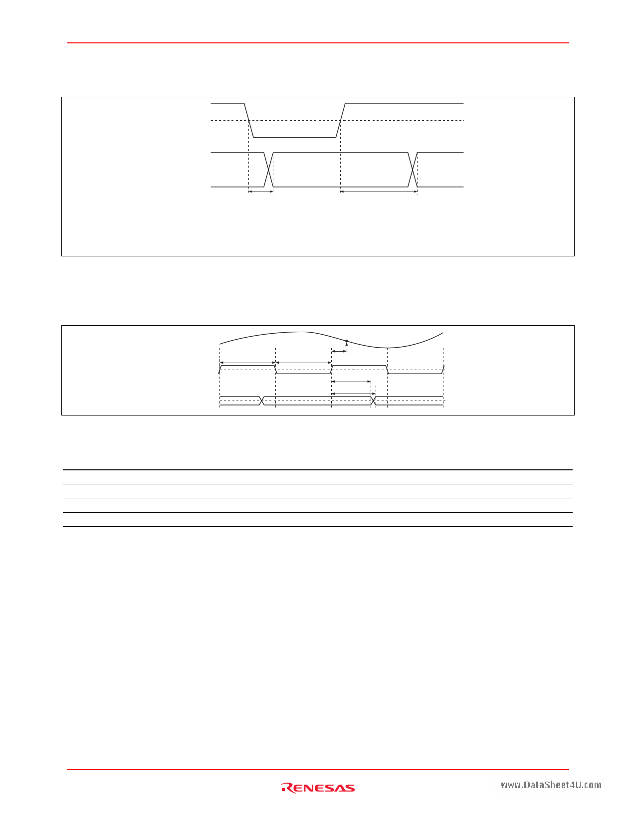
Detailed Timing Specifications at Pre-Blanking
Figure 5 shows the pre-blanking detailed timing specifications.
PBLK
Vth
www.DataSheet4U.com
Digital output ADC
(D0 to D9) data
Clamp level
ADC
data
VOH
tPBLK
ADCLK × 2 clocks
VOL
ADCLK × 10 clocks
(shifts one clock cycle depending
on the PBLK input timing)
When serial data SPinv bit is set to low
(When the SPinv is set to high, the PBLK polarity is inverted.)
Figure 5 Detailed Timing Specifications at Pre-Blanking
Detailed Timing Specifications when ADCIN Input Mode is Used
Figure 6 shows the detailed timing chart when ADCIN input mode is used, and table 9 shows each timing specification.
ADCIN
ADCLK
D0 to D9
(2)
(1)
(3)
(4)
(5)
Vth
VDD/2
Figure 6 Detailed Timing Chart when ADCIN Input Mode is Used
Table 9 Timing Specifications when ADCIN Input Mode is Used
No.
(1)
(2), (3)
(4)
(5)
Timing
Signal fetch time
ADCLK tWH min./tWL min.
ADCLK rising to digital output hold time
ADCLK rising to digital output delay time
Symbol
tADC1
tADC2, 3
tAHLD4
tAOD5
Min
—
Typ × 0.85
10
—
Typ
(6)
1/2fADCLK
14.5
23.5
Max
—
Typ × 1.15
—
31.5
Unit
ns
ns
ns
ns
Rev.1.0 Apr 20, 2004 page 11 of 21
11 Page | ||
| Páginas | Total 22 Páginas | |
| PDF Descargar | [ Datasheet HD49340HNP.PDF ] | |
Hoja de datos destacado
| Número de pieza | Descripción | Fabricantes |
| HD49340HNP | CDS/PGA & 10-bit A/D Converter | Renesas Technology |
| Número de pieza | Descripción | Fabricantes |
| SLA6805M | High Voltage 3 phase Motor Driver IC. |
Sanken |
| SDC1742 | 12- and 14-Bit Hybrid Synchro / Resolver-to-Digital Converters. |
Analog Devices |
|
DataSheet.es es una pagina web que funciona como un repositorio de manuales o hoja de datos de muchos de los productos más populares, |
| DataSheet.es | 2020 | Privacy Policy | Contacto | Buscar |
