|
|
|
PDF SC2602L Data sheet ( Hoja de datos )
| Número de pieza | SC2602L | |
| Descripción | Synchronous Voltage Mode Controller | |
| Fabricantes | Semtech Corporation | |
| Logotipo | ||
Hay una vista previa y un enlace de descarga de SC2602L (archivo pdf) en la parte inferior de esta página. Total 14 Páginas | ||
|
No Preview Available !
SC2602L
Synchronous Voltage Mode Controller
for Distributed Power Supply
POWER MANAGEMENT
Description
Features
The SC2602L is low-cost, full featured, synchronous volt-
age-mode controller designed for use in single ended
power supply applications where efficiency is of primary
concern. Synchronous operation allows for the elimina-
tion of heat sinks in many applications. The SC2602L is
ideal for implementing DC/DC converters needed to
power advanced microprocessors in low cost systems,
or in distributed power applications where efficiency is
www.DataiSmhepeot4rUta.cnotm. Internal level-shift, high-side drive circuitry, and
preset shoot-through control, allows the use of inexpen-
sive N-channel power MOSFETs.
Synchronous operation for high efficiency (95%)
RDS(ON) current sensing
Output voltage can be programmed as low as 0.8V
On-chip power good and OVP functions
Small size with minimum external components
Soft Start
Enable function
SO-14 package is fully WEEE and RoHS compliant
Applications
SC2602L features include temperature compensated
voltage reference, triangle wave oscillator and current
sense comparator circuitry. Power good signaling, shut-
down, and over voltage protection are also provided.
The SC2602L operates at a fixed 200kHz which is for
optimum compromise between efficiency, external com-
ponent size, and cost.
Microprocessor core supply
Low cost synchronous applications
Voltage Regulator Modules (VRM)
DDR termination supplies
Networking power supplies
Sequenced power supplies
Two SC2602L can be used together to sequence two
voltage regulators for power up in telecom systems. The
power good of the first SC2602L connected to the en-
able of the second SC2602L makes this possible.
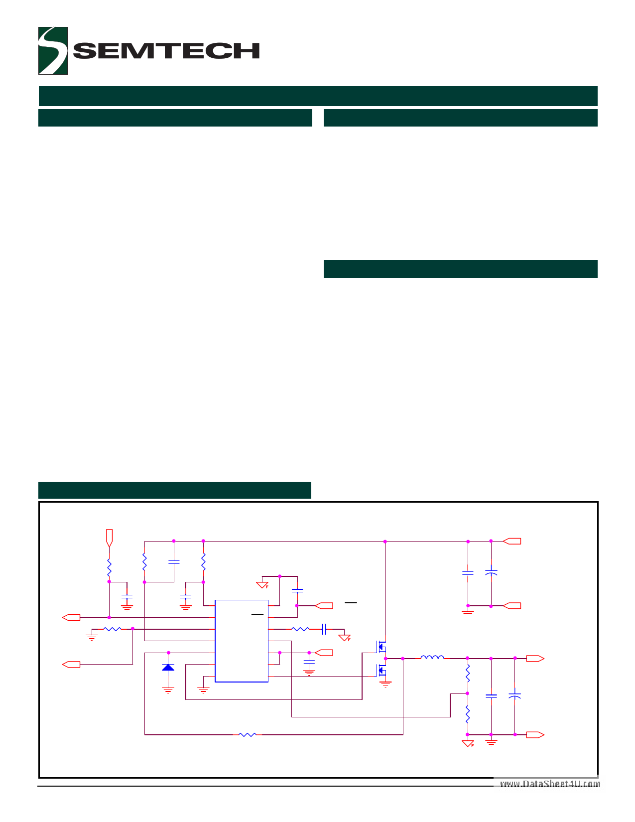
Typical Application Circuit
V_pullup
PWRGD
OVP
R1 R2
R3 C1
C5
R4
U1
C6 1
VCC
14
GND
2 PWRGD SS/SHDN 13
3 OVP
COMP 12
4 OCSET
SENSE 11
5 PHASE
BSTH 10
6 DH
BSTL 9
D1 7
8
PGND
DL
SC 2602L
C4
SS/ SH D N
R5 C7
12V IN
C8
Q1
L1
Q2
R8
Figure 1. Typical distributed power supply
Revision: January 05, 2006
1
5V IN
+
C3 C2
GND
R6 2.5V OUT
+
C10 C9
R7
GND
www.semtech.com
1 page 
SC2602L
POWER MANAGEMENT
Block Diagram
VCC
PWRGD
OVP
SENSE
www.DataSheet4U.com
COMP
VCC
SS/SHDN
GND
+10%
-10%
0.8V
+20%
Vbg
Error Amp
Vbg
VCC
10uA
1.5uA
0.8V
0.6V
Under
Voltage
Oscillator
One Shot
PWM
S
R QB
Fault
Over Current
200uA
DRVH
Cross
Current
Control
DRVL
OCSET
BSTH
DH
PHASE
BSTL
DL
PGND
Theory of Operation
Synchronous Buck Converter
The output rail is regulated by a synchronous, voltage-
mode pulse width modulated (PWM) controller. This
section has all the features required to build a high effi-
ciency synchronous buck converter, including “Power
Good” flag, shut-down, and cycle-by-cycle current limit.
The output voltage of the synchronous converter is set
and controlled by the output of the error amplifier. The
external resistive divider reference voltage is derived from
an internal trimmed-bandgap voltage reference (See Fig.
1). The inverting input of the error amplifier receives its
voltage from the SENSE pin.
The internal oscillator uses an on-chip capacitor and
trimmed precision current sources to set the oscillation
frequency to 200kHz. The triangular output of the oscil-
lator sets the reference voltage at the inverting input of
the comparator. The non-inverting input of the compara-
tor receives it’s input voltage from the error amplifier.
When the oscillator output voltage drops below the er-
ror amplifier output voltage, the comparator output goes
high. This pulls DL low, turning off the low-side FET, and
DH is pulled high, turning on the high-side FET (once
the cross-current control allows it). When the oscillator
voltage rises back above the error amplifier output volt-
age, the comparator output goes low. This pulls DH low,
turning off the high-side FET, and DL is pulled high, turn-
ing on the low-side FET (once the cross-current control
allows it).
As SENSE increases, the output voltage of the error
amplifier decreases. This causes a reduction in the on-
time of the high-side MOSFET connected to DH, hence
lowering the output voltage.
Under Voltage Lockout
The under voltage lockout circuit of the SC2602L as-
sures that the high-side MOSFET driver outputs remain
in the off state whenever the supply voltage drops below
set parameters. Lockout occurs if VCC falls below 4.1V.
Normal operation resumes once VCC rises above 4.2V.
Over-Voltage Protection
The over-voltage protection pin (OVP) is high only when
the voltage at SENSE is 20% higher than the target value
programmed by the external resistor divider. The OVP
pin is internally connected to a PNP’s collector.
Power Good
The power good function is to confirm that the regulator
outputs are within +/-10% of the programmed level.
PWRGD remains high as long as this condition is met.
PWRGD is connected to an internal open collector NPN
transistor.
2005 Semtech Corp.
5
www.semtech.com
5 Page 
SC2602L
POWER MANAGEMENT
Gpwm
EA
Vbg
1.25Vdc
0.85Vddcc
R
Vin
C
The task here is to properly choose the compensation
L network for a nicely shaped loop-gain Bode plot. The
following design procedures are recommended to ac-
R1 complish the goal:
Rc
Ro
Co R2
(1) Calculate the corner frequency of the output filter:
F o :=
1
2⋅π⋅ L⋅C o
Fig. 2. SC2602L small signal model.
www.DataTShheeetc4oUn.ctormol model of SC2602L control loop small signal
can be depicted in Fig. 2. This model can also be used in
SPICE kind of simulator to generate loop gain Bode plots.
The bandgap reference is 0.8V and trimmed to +/-1%
accuracy. The desired output voltage can be achieved
by setting the resistive divider network, R1 and R2.
The error amplifier is transconductance type with fixed
gain of:
Gm
1.8.mA
V
The compensation network includes a resistor and a
capacitor in series, which terminates from the output of
the error amplifier to the ground.
(2) Calculate the ESR zero frequency of the output filter
capacitor:
F esr
:=
1
2⋅π⋅R c⋅C o
(3) Check that the ESR zero frequency is not too high.
F esr
<
F sw
5
If this condition is not met, the compensation structure
may not provide loop stability. The solution is to add
some electrolytic capacitors to the output capacitor bank
to correct the output filter corner frequency and the ESR
zero frequency. In some cases, the filter inductance
may also need to be adjusted to shift the filter corner
frequency. It is not recommended to use only high fre-
quency multi-layer ceramic capacitors for output filter.
This device uses voltage mode control with input volt-
age feed forward. The peak-to-peak ramp voltage is
proportional to the input voltage, which results in an ex-
cellent performance to reject input voltage variation. The
PWM gain is inversion of the ramp amplitude, and this
gain is given by:
G pwm
1
V ramp
where the ramp amplitude (peak-to-peak) is 1.0 volts
when input voltage is 12 volts.
The total control loop-gain can then be derived as
follows:
T( s)
T o.
1 s.R.C .
s. R. C
1
1 s.R c.C o
s. R c.C o
L
Ro
s2.L.C o. 1
Rc
Ro
(4) Choose the loop gain cross over frequency (0 dB
frequency). It is recommended that the crossover fre-
quency is always less than one fifth of the switching
frequency :
F x_over ≤
F sw
5
If the transient specification is not stringent, it is better to
choose a crossover frequency that is less than one tenth
of the switching frequency for good noise immunity. The
resistor in the compensation network can then be cal-
culated as:
R
:=
G
1
pwm ⋅ V
in⋅G
m
⋅
F esr
Fo
2
⋅
F
x_over
⋅
F esr
Vo
V bg
when
T
o
:=
G m⋅G pwm⋅V
in⋅R⋅
V bg
Vo
F o < F esr < F x_over
2005 Semtech Corp.
11
www.semtech.com
11 Page | ||
| Páginas | Total 14 Páginas | |
| PDF Descargar | [ Datasheet SC2602L.PDF ] | |
Hoja de datos destacado
| Número de pieza | Descripción | Fabricantes |
| SC2602 | Synchronous Voltage Mode Controller | Semtech Corporation |
| SC2602A | Synchronous Voltage Mode Controller | Semtech Corporation |
| SC2602L | Synchronous Voltage Mode Controller | Semtech Corporation |
| Número de pieza | Descripción | Fabricantes |
| SLA6805M | High Voltage 3 phase Motor Driver IC. |
Sanken |
| SDC1742 | 12- and 14-Bit Hybrid Synchro / Resolver-to-Digital Converters. |
Analog Devices |
|
DataSheet.es es una pagina web que funciona como un repositorio de manuales o hoja de datos de muchos de los productos más populares, |
| DataSheet.es | 2020 | Privacy Policy | Contacto | Buscar |