|
|
|
PDF HFBR-789BHZ Data sheet ( Hoja de datos )
| Número de pieza | HFBR-789BHZ | |
| Descripción | Pluggable Parallel Fiber Optic Modules | |
| Fabricantes | AVAGO TECHNOLOGIES | |
| Logotipo | ||
Hay una vista previa y un enlace de descarga de HFBR-789BHZ (archivo pdf) en la parte inferior de esta página. Total 22 Páginas | ||
|
No Preview Available !
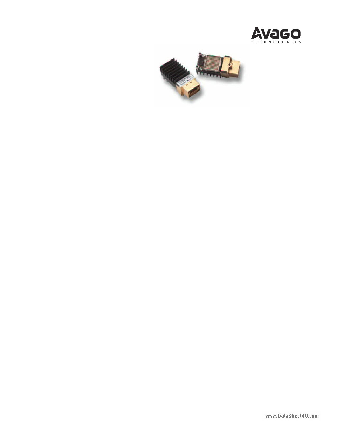
HFBR-779BZ/BEZ/BHZ and HFBR-789BZ/BEZ/BHZ
Pluggable Parallel Fiber Optic Modules, Transmitter and Receiver
www.DataSheet4U.com
Data Sheet
Description
The HFBR-779BZ transmitter and HFBR-789BZ
receiver are high performance fiber optic modules
for parallel optical data communication
applications. These 12-channel devices, operating
up to 2.7 Gbd per channel, provide a cost
effective solution for short-reach applications
requiring up to 32 Gb/s aggregate bandwidth.
These modules are designed to operate on
multimode fiber systems at a nominal wavelength
of 850 nm. They incorporate high performance,
highly reliable, short wavelength optical devices
coupled with proven circuit technology to provide
long life and consistent service.
The HFBR-779BZ transmitter module incorporates
a 1 2 - channel VCSEL (Vertical Cavity Surface
Emitting Laser) array together with a custom
12-channel laser driver integrated circuit
providing IEC-60825 and CDRH Class 1M laser
eye safety.
The HFBR-789BZ receiver module contains a
12-channel PIN photodiode array coupled with
a custom preamplifier / post amplifier integrated
circuit.
Operating from a single +3.3 V power supply,
both modules provide LVTTL or LVCMOS control
interfaces and Current Mode Logic (CML)
compatible data interfaces to simplify external
circuitry.
The transmitter and receiver devices are housed
in MTP®/MPO receptacled packages. Electrical
connections to the devices are achieved by
means of a pluggable 10 x 10 connector array.
Features
• RoHS Compliant
• Low cost per Gb/s
• High package density per Gb/s
• 3.3 volt power supply for low power consumption
• 850 nm VCSEL array source
• 12 independent channels per module
• Separate transmitter and receiver modules
• 2.7 Gbd data rate per channel
• Standard MTP® (MPO) ribbon fiber connector
interface
• Pluggable package
• 62.5/125 micron multimode fiber operation:
Distance up to 100 m with 160 MHz.km fiber at 2.5 Gbd
Distance up to 200 m with 400 MHz.km fiber at 2.5 Gbd
• Data I/O is CML compatible
• Control I/O is LVTTL compatible
• Manufactured in an ISO 9002 certified facility
Applications
• Datacom switch and router backplane connections
• Telecom switch and router backplane connections
Ordering Information
The HFBR-779BZ and HFBR-789BZ products
are available for production orders through the
Avago Technologies Component Field Sales office.
HFBR-779BZ No EMI Nose Shield
HFBR-789BZ No EMI Nose Shield
HFBR-779BEZ With Extended EMI Nose Shield
HFBR-789BEZ With Extended EMI Nose Shield
HFBR-779BHZ No EMI Nose Shield, No Heatsink
HFBR-789BHZ No EMI Nose Shield, No Heatsink
1 page 
Absolute Maximum Ratings [1,2]
www.DataSheet4U.com
Parameter
Symbol
Min.
Max.
Unit Reference
Storage Temperature (non-operating)
TS
–40 100 °C 1
Case Temperature (operating)
TC
90 °C 1, 2, 4
Supply Voltage
VCC –0.5 4.6 V 1, 2
Data/Control Signal Input Voltage
VI
–0.5
VCC + 0.5
V
1
Transmitter Differential Data Input Voltage |VD|
2 V 1, 3
Output Current (dc)
ID
25 mA 1
Relative Humidity (non-condensing)
RH
5
95 % 1
Notes:
1. Absolute Maximum Ratings are those values beyond which damage to the device may occur. See Reliability Data Sheet for specific reliability
performance.
2. Between Absolute Maximum Ratings and the Recommended Operating Conditions functional performance is not intended, device reliability is not
implied, and damage to the device may occur over an extended period of time.
3. This is the maximum voltage that can be applied across the Transmitter Differential Data Inputs without damaging the input circuit.
4. Case Temperature is measured as indicated in Figure 3.
Recommended Operating Conditions [1]
Parameter
Symbol
Min.
Typ.
Max. Unit Reference
Case Temperature
Supply Voltage
Signaling Rate per Channel
TC
VCC
0
3.135
1
40
3.3
80 °C 2, Figs. 3, 4
3.465
V
Figs. 5, 6, 12
2.72 Gbd 3
Data Input Differential Peak-to-Peak
Voltage Swing
DVDINP-P
175
1400
mVP-P
4, Figs. 7, 8
Control Input Voltage High
Control Input Voltage Low
Power Supply Noise for
Transmitter and Receiver
VIH
VIL
NP
2.0
VEE
VCC V
0.8 V
200
mVP-P
5, Figs. 5, 6
Transmitter/Receiver Data
I/O Coupling Capacitors
Receiver Differential Data Output Load
CAC
RDL
0.1 µF Fig. 7
100 W Fig. 7
Notes:
1. Recommended Operating Conditions are those values outside of which functional performance is not intended, device reliability is not implied, and
damage to the device may occur over an extended period of time. See Reliability Data Sheet for specific reliability performance.
2. Case Temperature is measured as indicated in Figure 3. A 55°C, 1 m/s, parallel to the printed circuit board, air flow at the module or equivalent
cooling is required. See Figure 4.
3. The receiver has a lower cut off frequency near 100 kHz.
4. Data inputs are CML compatible. Coupling capacitors are required to block DC. ∆VDINP-P = ∆VDINH – ∆VDINL, where ∆VDINH = High State Differential
Data Input Voltage and ∆VDINL = Low State Differential Data Input Voltage.
5. Power Supply Noise is defined for the supply, VCC, over the frequency range from 500 Hz to 2500 MHz, with the recommended power supply filter
in place, at the supply side of the recommended filter. See Figures 5 and 6 for recommended power supply filters.
5
5 Page 
Table 1. Transmitter Module Pad Description
www.DataSheet4U.com
Symbol
Functional Description
VEE Transmitter Signal Common. All voltages are referenced to this potential unless otherwise indicated. Directly
connect these pads to transmitter signal ground plane.
VCCT
DIN0+ through DIN11+
Transmitter Power Supply. Use recommended power supply filter circuit in Figure 6.
Transmitter Data In+ for channels 0 through 11, respectively. Differential termination and self bias are included,
see Figure 11.
DIN0– through DIN11–
Transmitter Data In- for channels 0 through 11, respectively. Differential termination and self bias are included;
see Figure 11.
TX_EN
TX_DIS
RESET-
TX Enable. Active high. Internal pull-up High = VCSEL array is enabled if TX_DIS is inactive (Low). Low =
VCSEL array is off. TX_EN must be taken to a logic low state level (VOL) for 1 ms or longer.
TX Disable. Active high. Internal pull-down Low = VCSEL array is enabled if TX_EN is active (High). High =
VCSEL array is off. TX_DIS must be taken to a logic High state level (VOH) for 1 ms or longer.
Transmitter RESET- input. Active low. Internal pull-up. Low = Resets logic functions, clears FAULT- signal,
VCSEL array is off. High = Normal operation. See Figure 14.
FAULT-
Transmitter FAULT- output. Active low. Low (logic "0") results from a VCSEL over-current condition, out of
temperature range, or EEPROM calibration data corruption condition detected for any VCSEL. An asserted (logic
"0") FAULT- disables the VCSEL array and is cleared by RESET- or power cycling VCCT FAULT- is a single ended
LVTTL compatible output.
DNC Do not connect to any electrical potential.
Table 2. Receiver Module Pad Description
Symbol
Functional Description
VEE
VCCR
VPP
DOUT0+ through DOUT11+
DOUT0– through DOUT11–
SD
RX_EN
SQ_EN
EN_SD
DNC
Receiver Signal Common. All voltages are referenced to this potential unless otherwise indicated.
Directly connect these pads to receiver signal ground plane.
Receiver Power Supply. Use recommended power supply filter circuit in Figure 5.
Not required for Avago Technologies product. Pads not internally connected.
(Voltage for MSA compatibility in order to ac-couple receiver data outputs).
Receiver Data Out+ for channels 0 through 11, respectively. Terminate these high-speed differential CML outputs
with standard CML techniques at the inputs of the receiving device. Individual data outputs will be squelched for
insufficient input signal level.
Receiver Data Out- for channel 0 through 11, respectively. Terminate these high-speed differential CML outputs
with standard CML techniques at the inputs of the receiving device. Individual data outputs will be squelched for
insufficient input signal level.
Signal Detect. Normal optical input levels to all channels results in a logic "1" output, VOH, asserted. Low input
optical levels to any channel results in a fault condition indicated by a logic "0" output, VOL, de-asserted. SD is a
single-ended LVTTL compatible output.
Receiver output enable. Active high (logic "1"), internal pull-up. Low (logic "0") = receiver outputs disabled, all
outputs are high (logic "1").
Squelch enable input. Active high (logic "1"), internal pull-up. Low (logic "0") = squelch disabled.
When SQ_EN is high and SD is low, corresponding outputs are squelched.
Enable Signal Detect. Active high (logic "1"), internal pull-up. Low (logic "0") = Signal detect output forced
active high.
Do not connect to any electrical potential.
11
11 Page | ||
| Páginas | Total 22 Páginas | |
| PDF Descargar | [ Datasheet HFBR-789BHZ.PDF ] | |
Hoja de datos destacado
| Número de pieza | Descripción | Fabricantes |
| HFBR-789BHZ | Pluggable Parallel Fiber Optic Modules | AVAGO TECHNOLOGIES |
| Número de pieza | Descripción | Fabricantes |
| SLA6805M | High Voltage 3 phase Motor Driver IC. |
Sanken |
| SDC1742 | 12- and 14-Bit Hybrid Synchro / Resolver-to-Digital Converters. |
Analog Devices |
|
DataSheet.es es una pagina web que funciona como un repositorio de manuales o hoja de datos de muchos de los productos más populares, |
| DataSheet.es | 2020 | Privacy Policy | Contacto | Buscar |