|
|
|
PDF NJW4124 Data sheet ( Hoja de datos )
| Número de pieza | NJW4124 | |
| Descripción | Lithium-Battery Charger Controller IC with Timer / DMP20 | |
| Fabricantes | JRC | |
| Logotipo | ||
Hay una vista previa y un enlace de descarga de NJW4124 (archivo pdf) en la parte inferior de esta página. Total 20 Páginas | ||
|
No Preview Available !
www.DataSheet4U.com
NJW4124
Lithium-ion Battery Charger Controller IC with Timer
■GENERAL DESCRIPTION
NJW4124 is a 1-cell and 2-cell lithium ion battery charge control IC
with a built-in AC-DC secondary side control feature. Using a
photocoupler to directly feed back optimum charging voltage and
current information to the primary side, it increases energy
efficiency, makes possible a smaller charger, and conserves
energy. Charging current can be freely set and therefore it is
possible to optimize charging according to battery capacity.
As safety features it has over voltage, over discharge, temperature
detection, and a charge over timer. Also, the adaptor and the
charge control circuit are mounted on one chip.
■FEATURES
● Charge Control Feedback by Photocoupler
● Adjustable Charge Voltage
● Adjustable Pre-Charge and Full Charge Current
● Temperature Monitor
● Over Charge Timer
● Internal Re-Charge function
● Delay timers and Hysteresis inputs for high noise immunity
● Over Discharge Battery Detect
● Over Voltage Protection
● Bi-CMOS Technology
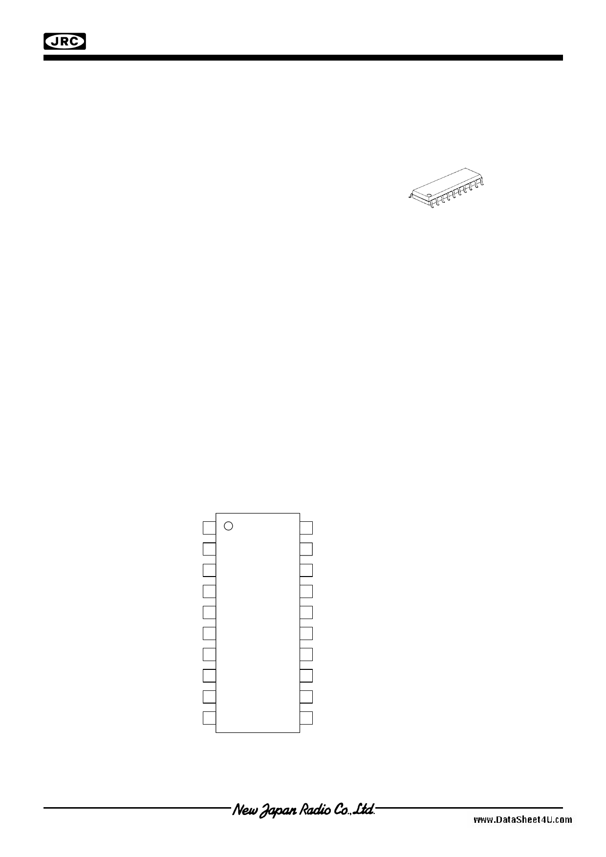
● Package Outline
NJW4124M : DMP20
■PIN CONFIGURATION
P-CHG 1
NFB
TX-SW
2
3
GND
4
PC 5
ADP
LED-G
LED-R
6
7
8
C1 9
C2 10
20 Q-CHG
19 CS1
18 CS2
17 VS
16 VREF
15 V+
14 TDET
13 TH
12 TL
11 CHG-SW
■PACKAGE OUTLINE
NJW4124M
NJW4124M
Ver.2006-01-18
-1-
1 page 
www.DataSheet4U.com
NJW4124
■PIN CONFIGULATION
Pin No.
Pin Name
1 P-CHG
2 NFB
3 TX-SW
4 GND
5 PC
6 ADP
7 LED-G
8 LED-R
9 C1
10 C2
11 CHG-SW
12 TL
13 TH
14 TDET
15 V+
16 VREF
17 VS
18 CS2
19 CS1
20 Q-CHG
Function
Pre-Charge Current Setting
Current-Regulation-Loop Compensation
Switch Transistor connection
GND
Photocoupler connection for the first side feedback
Adaptor Control Voltage Setting
LED Output
LED Output
Pre-Charge Timer, 2mA Charge Timer, LED Blinking Cycle, Delay Time Setting
Quick Timer Setting
Charge ON/OFF Control
Batteries Thermal (High Temperature) Setting
Batteries Thermal (Low Temperature) Setting
Battery Temperature Detection, Battery Connected Detection
Operating Voltage
Reference Voltage Output
Battery Voltage Detection
Charge Current Detection 2
Charge Current Detection 1
Quick Charge Current Setting
■CHARGE VOLTAGE / CURRENT for RESISTANCE SETTING
Parameter
Calculation formula
Adaptor Output Voltage
VADP
=
RA1 + RA2
RA 2
x
VREF-ADP (1.24V)
Charge Control Voltage
VBAT
=
RB1 + RB2
RB2
x
VREF-CV (2.1V)
Low Voltage Detection
Voltage
VBAT x 0.525
Quick Charge Start Voltage
Re-Charge Detection Voltage
Over Voltage Detection
Voltage
VBAT x 0.73
VBAT x 0.95
VBAT x 1.025
Pre-Charge Current
Quick Charge Current
Full Charge Current
IP-CHG =
(
RP2
RP1 + RP2
x
VREF (1.24V)
/
4)
/
RCS
(at. RP1:232kΩ, RP2:16kΩ, RCS=0.2Ω)
IQ-CHG =
(
RQ2
RQ1 + RQ2
x
VREF (1.24V)
/
4)
/
RCS
(at. RQ1:128kΩ, RQ2:120kΩ, RCS=0.2Ω)
IF-CHG = (96mV / 8) / RCS
(at. RCS=0.2Ω)
Examples of calculation
5.0V 10V
4.2V 8.4V
2.21V
3.07 V
3.99 V
4.305 V
4.41V
6.13 V
7.98 V
8.61 V
100mA
750mA
60mA
Ver.2006-01-18
-5-
5 Page 
NJW4124
www.DataSheet4U.com
■FEATURE DESCRIPTION (CONTINUED)
3. Current Detection Block (CS1 pin, CS2 pin)
A current detection resistor RCS is inserted between pin CS1 and pin CS2 to monitor battery charge current.
The input voltage between pin CS1 and pin CS2 is amplified by the 12dB current detection amp and fed back to the charge
current control amp. (Figure 4)
3-1. Pre-Charge Current, Quick Charge Current (P-CHG pin, Q-CHG pin)
This will switch between charging with pre-charge current or quick charge current according to the level of the battery
voltage VBAT that is input from the VS pin.
VBAT x 0.525 to VBAT x 0.73
VBAT x 0.73 to VBAT
Pre-charge control
Quick charge control
Pre-charge and quick charge current values are determined by the P-CHG pin and the Q-CHG pin voltage settings.
Settings are made according to the following formulae.
Pre-Charge Current Value
IP-CHG =
( RP2
RP1 + RP2
x
VREF (1.24V)
/
4)
/
RCS
PC
NFB P-CHG
RP1
VREF
RQ1
RP2 RQ2
Q-CHG
Quick Charge Current Value
IQ-CHG =
(
RQ2
RQ1 + RQ2
x
VREF (1.24V)
/
4)
/
RCS
To OR
Circuit
Charge Current
Control Amp
12dB
CS1
Rcs
3-2. Full Charge Detection (F-CHG pin)
Charge termination is determined by a set full
charge current IF-CHG., which is determined by a
voltage setting on the F-CHG pin.
IF-CHG = (96mV/ 8) / RCS
When charging is terminated, LED-G turns on,
and the sequence moves to the re-charge
detection operation.
CVCC-ON
Quick/
Pre-Charge
Control Block
To Charge Voltage
Control Amp
Switch Pre/Quick
Charge Current
Full Charge
Detection
6dB
Quick Charge
Detection
VBAT x 0.73
CS2
VS
RB1
RB2
To Charge
Output
Figure 4. Block for Controlling Pre-Charge, Quick Charge,
and Block for Detecting Full Charge.
Ver.2006-01-18
- 11 -
11 Page | ||
| Páginas | Total 20 Páginas | |
| PDF Descargar | [ Datasheet NJW4124.PDF ] | |
Hoja de datos destacado
| Número de pieza | Descripción | Fabricantes |
| NJW4120 | Lithium-Battery Charger Controller IC with Timer / DMP20 / SSOP20 | JRC |
| NJW4124 | Lithium-Battery Charger Controller IC with Timer / DMP20 | JRC |
| NJW4128 | Switching Regulator IC | New Japan Radio |
| Número de pieza | Descripción | Fabricantes |
| SLA6805M | High Voltage 3 phase Motor Driver IC. |
Sanken |
| SDC1742 | 12- and 14-Bit Hybrid Synchro / Resolver-to-Digital Converters. |
Analog Devices |
|
DataSheet.es es una pagina web que funciona como un repositorio de manuales o hoja de datos de muchos de los productos más populares, |
| DataSheet.es | 2020 | Privacy Policy | Contacto | Buscar |