|
|
|
PDF AS28F128J3M Data sheet ( Hoja de datos )
| Número de pieza | AS28F128J3M | |
| Descripción | Plastic Encapsulated Microcircuit 128Mb | |
| Fabricantes | Austin Semiconductor | |
| Logotipo | ||
Hay una vista previa y un enlace de descarga de AS28F128J3M (archivo pdf) en la parte inferior de esta página. Total 8 Páginas | ||
|
No Preview Available !
Austin Semiconductor, Inc.
PEM
AS28F128J3M
Q-Flash
Plastic Encapsulated Microcircuit
128Mb, x8 and x16 Q-FLASH Memory
Even Sectored, Single Bit per Cell Architecture
Features
• 100% Pin and Function compatible to Intel’s MLC Family
• NOR Cell Architecture
• 2.7V to 3.6V VCC
• 2.7V to 3.6V or 5V VPEN (Programming Voltage)
• Asynchronous Page Mode Reads
• Manufacturer’s ID Code:
! MT28F128J3MRG
Micron
0x2Ch
• Industry Standard Pin-Out
• Fully compatible TTL Input and Outputs
• Common Flash Interface [CFI]
• Scalable Command Set
• Automatic WRITE and ERASE Algorithms
• 5.6us per Byte effective programming time
• 128 bit protection register
! 64-bit unique device identifier
! 64-bit user programmable OTP cells
• Enhanced data protection feature with use of VPEN=VSS
• Security OTP block feature
• 100,000 ERASE cycles per BLOCK
• Automatic Suspend Options:
! Block ERASE SUSPEND-to-READ
! Block ERASE SUSPEND-to-PROGRAM
! PROGRAM SUSPEND-to-READ
• Available Operating Ranges:
www.Da!taShEeneht4aUn.cceodm
[-ET] -40oC to +105oC
! Mil-Temperature [-XT] -55oC to +125oC
For in-depth functional product detail and Timing Diagrams,
please reference Micron’s full product Datasheet:
MT28F640J3 Rev. L Dated 04/16/04
General Description
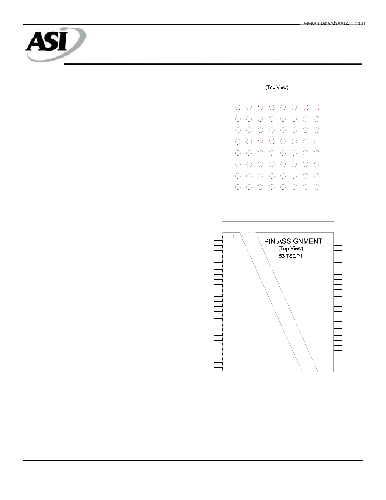
PIN ASSIGNMENT
123 456 78
A
A1 A6
A8 VPEN A13 VCC A18 A22
B
A2 VSS A9 CE0 A14 A25 A19 CE1
C
A3
A7 A10 A12 A15 DNU A20 A21
D
A4 A5 A11 RP\ DNU DNU A16 A17
E
DQ8 DQ1 DQ9 DQ3 DQ4 DNU DQ15 STS
F
BYTE\ DQ0 DQ10 DQ11 DQ12 DNU DNU OE\
G
A23
A0 DQ2 VCCQ DQ5 DQ6 DQ14 WE\
H
CE2 DNU VCC VSS DQ13 VSS DQ7 A24
64-Ball FBGA
A22
CE1
A21
A20
A19
A18
A17
A16
VCC
A15
A14
A13
A12
CE0
VPEN
RP\
A11
A10
A9
A8
VSS
A7
A6
A5
A4
A3
A2
A1
1
2
3
4
5
6
7
8
9
10
11
12
13
14
15
16
17
18
19
20
21
22
23
24
25
26
27
28
56 NC
55 WE\
54 OE\
53 STS
52 DQ15
51 DQ7
50 DQ14
49 DQ6
48 VSS
47 DQ13
46 DQ5
45 DQ12
44 DQ4
43 VCCQ
42 VSS
41 DQ11
40 DQ3
39 DQ10
38 DQ2
37 VCC
36 DQ9
35 DQ1
34 DQ8
33 DQ0
32 A0
31 BYTE\
30 A23
29 CE2
ASI’s, AS28F128J3M Enhanced or Mil-Temp variant of Micron’s This device features in-system block locking. They also have a
Q-Flash family of devices, is a nonvolatile, electrically block- Common FLASH Interface [CFI] that permits software algorithms
erasable (FLASH), programmable memory device manufactured to be used for entire families of devices. The software is device-
using Micron’s 0.15um process technology. This device independent, JEDEC ID-independent with forward and backward
containing 134,217,728 bits organized as either 16,777,218 (x8) compatibility.
or 8,388,608 bytes (x16). The device is uniformly sectored with
one hundred and twenty eight 128KB ERASE blocks.
AS28F128J3MRG
Revision 5.0 11/23/04
Austin Semiconductor, Inc. reserves the right to change products or modify product specifications with appropriate notification
For Additional Products and Information visit out Web site at www.austinsemiconductor.com
1
1 page 
Austin Semiconductor, Inc.
PEM
AS28F128J3M
Q-Flash
Memory Command Set Operations:
Command
READ ARRAY
READ IDENTIFIER CODES
READ QUERY
READ STATUS REGISTER
CLEAR STATUS REGISTER
WRITE TO BUFFER
WORD/BYTE PROGRAM
BLOCK ERASE
BLOCK ERASE/PROGRAM
SUSPEND
BLOCK ERASE/PROGRAM
RESUME
CONFIGURATION
SET BLOCK LOCK BITS
CLEAR BLOCK LOCK BITS
PROTECTION PROGRAM
Scalable or Basic Command
Set [SCS or BCS]
SCS / BCS
SCS / BCS
SCS
SCS / BCS
SCS / BCS
SCS / BCS
SCS / BCS
SCS / BCS
SCS / BCS
First Bus Cycle
Bus Cycles Operation Address
Data
1
>/= 2
WRITE
WRITE
X
X
FFh
90h
WRITE
X
98h
2 WRITE X
70h
1 WRITE X
50h
>2 WRITE BA
E8h
2 WRITE X 40h or 10h
2
WRITE
BA
20h
1 WRITE X
B0h
Second Bus Cycle
Operation Address
Data
READ
READ
READ
IA
QA
X
ID
QD
SRD
WRITE
WRITE
WRITE
BA
PA
BA
N
PD
D0h
SCS / BCS
1 WRITE X
D0h
SCS
SCS
SCS
2 WRITE X
2 WRITE X
2 WRITE X
2 WRITE X
B8h WRITE
60h WRITE
60h WRITE
C0h WRITE
X
BA
X
PA
CC
01h
D0h
PD
Notes
1
2
3, 4, 5
6, 7
5, 6
7, 8
7
Key:
[IA]
[ID]
[BA]
[QA]
[PA]
[QD]
[SRD]
Identifier Code address
Data read from identifier Code
Address within a Block
Query data base Address
Address of Memory location to be programmed
Data read from Query data base
Data read from Status Register
Notes
[1]
[2]
[3]
[4]
[5]
[6]
[7]
www.DataSheet4[8U] .com
Following the READ IDENTIFIER CODES command, READ operations access manufacturer, device, and block lock codes.
If the ISM is running, only DQ7 is valid; DQ15-DQ8 and DQ6-DQ0 are placed in High-Z
After the WRITE-to-BUFFER command is issued, check the XSR to make sure a buffer is available for WRITING
The number of Bytes/words to be written to the write buffer = n+1, where n=byte/word count argument. Count ranges on this device
for byte mode are n=00H to n=1Fh and for word mode, n=0000h to 000Fh. The third and consecutive bus cycles, as determined by n,
are for writing data into the write buffer. The CONFIRM command (D0h) is expected after exactly n+1 WRITE cycles; any other
command at that point in the sequence aborts the WRITE-to-BUFFER operation.
The WRITE-to-BUFFER or ERASE operation does not begin until a CONFIRM command (D0h) is issued
Attempts to issue a BLOCK ERASE or PROGRAM to a locked block will fail
Etiher 40h or 10h is recognized by the ISM as the byte/word program setup
PROGRAM SUSPEND can be issued after either the WRITE-to-BUFFER or WORD/BYTE PROGRAM operation is inititated.
The CLEAR BLOCK LOCK BITS operation simultaneously clears all block lock bits.
AS28F128J3MRG
Revision 5.0 11/23/04
Austin Semiconductor, Inc. reserves the right to change products or modify product specifications with appropriate notification
For Additional Products and Information visit out Web site at www.austinsemiconductor.com
5
5 Page | ||
| Páginas | Total 8 Páginas | |
| PDF Descargar | [ Datasheet AS28F128J3M.PDF ] | |
Hoja de datos destacado
| Número de pieza | Descripción | Fabricantes |
| AS28F128J3A | x8 and x16 Q-FLASH Memory | Austin Semiconductor |
| AS28F128J3A | 128Mb x8 and x16 Q-FLASH Memory | Micross |
| AS28F128J3M | Plastic Encapsulated Microcircuit 128Mb | Austin Semiconductor |
| Número de pieza | Descripción | Fabricantes |
| SLA6805M | High Voltage 3 phase Motor Driver IC. |
Sanken |
| SDC1742 | 12- and 14-Bit Hybrid Synchro / Resolver-to-Digital Converters. |
Analog Devices |
|
DataSheet.es es una pagina web que funciona como un repositorio de manuales o hoja de datos de muchos de los productos más populares, |
| DataSheet.es | 2020 | Privacy Policy | Contacto | Buscar |