|
|
|
PDF WCMA1016U4X Data sheet ( Hoja de datos )
| Número de pieza | WCMA1016U4X | |
| Descripción | 64K x 16 Static RAM | |
| Fabricantes | Weida Semiconductor | |
| Logotipo | ||
Hay una vista previa y un enlace de descarga de WCMA1016U4X (archivo pdf) en la parte inferior de esta página. Total 11 Páginas | ||
|
No Preview Available !
1
WCMA1016U4X
Features
• High Speed
— 55ns and 70ns availability
• Low voltage range
— 2.7V−3.6V
• Ultra-low active power
• Low standby power
• Easy memory expansion with CE and OE features
• Automatic power-down when deselected
• CMOS for optimum speed/power
Functional Description
The WCMA1016U4X is a high-performance CMOS static
RAM organized as 64K words by 16 bits. This device features
advanced circuit design to provide ultra-low active current.
This device s ideal for portable applications such as cellular
telephones. The device also has an automatic power-down
feature that significantly reduces power consumption by 99%
when addresses are not toggling. The device can also be put
into standby mode when deselected (CE HIGH or both BLE
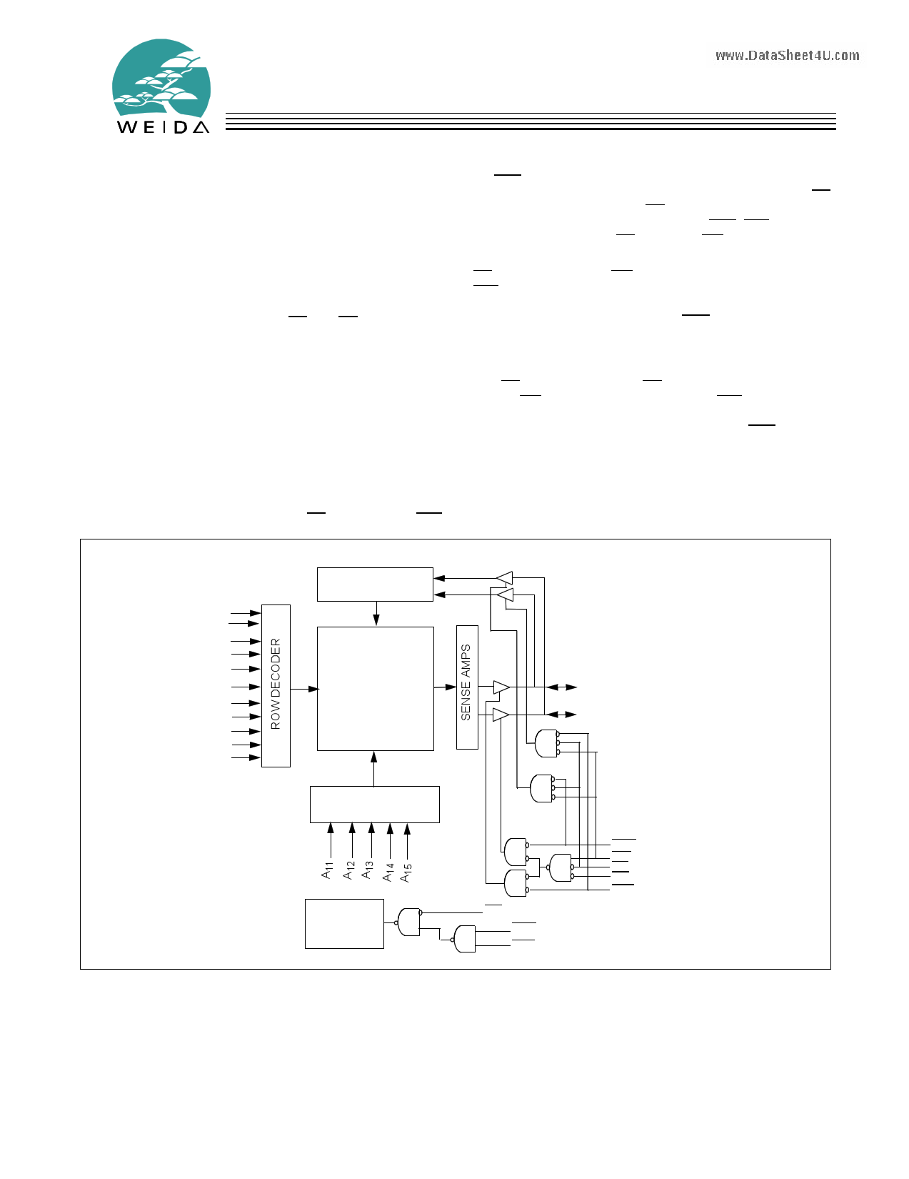
Logic Block Diagram
www.DataSheet4U.com
AA190
A8
A7
A6
A5
A4
A3
AA21
A0
DATA IN DRIVERS
64K x 16
RAM Array
2048 X 512
64K x 16 Static RAM
and BHE are HIGH). The input/output pins (I/O0 through I/O15)
are placed in a high-impedance state when: deselected (CE
HIGH), outputs are disabled (OE HIGH), both Byte High En-
able and Byte Low Enable are disabled (BHE, BLE HIGH), or
during a write operation (CE LOW, and WE LOW).
Writing to the device is accomplished by taking Chip Enable
(CE) and Write Enable (WE) inputs LOW. If Byte Low Enable
(BLE) is LOW, then data from I/O pins (I/O0 through I/O7), is
written into the location specified on the address pins (A0
through A15). If Byte High Enable (BHE) is LOW, then data
from I/O pins (I/O8 through I/O15) is written into the location
specified on the address pins (A0 through A15).
Reading from the device is accomplished by taking Chip En-
able (CE) and Output Enable (OE) LOW while forcing the Write
Enable (WE) HIGH. If Byte Low Enable (BLE) is LOW, then
data from the memory location specified by the address pins
will appear on I/O0 to I/O7. If Byte High Enable (BHE) is LOW,
then data from memory will appear on I/O8 to I/O15. See the
Truth Table at the back of this data sheet for a complete de-
scription of read and write modes.
The WCMA1016U4X is available in a 48-ball FBGA package.
I/O0–I/O7
I/O8–I/O15
COLUMN DECODER
Power -Down
Circuit
CE
BHE
BLE
BHE
WE
CE
OE
BLE
1 page 
WCMA1016U4X
Switching Characteristics Over the Operating Range[7]
WCMA1016U4X-55 WCMA1016U4X-70
Parameter
Description
Min.
Max.
Min.
Max.
Unit
READ CYCLE
tRC Read Cycle Time
tAA Address to Data Valid
tOHA
Data Hold from Address Change
tACE CE LOW to Data Valid
tDOE
tLZOE
tHZOE
tLZCE
tHZCE
OE LOW to Data Valid
OE LOW to Low Z[8]
OE HIGH to High Z[8, 9]
CE LOW to Low Z[8]
CE HIGH to High Z[8, 9]
tPU CE LOW to Power-Up
tPD CE HIGH to Power-Down
tDBE
BLE / BHE LOW to Data Valid
tLZBE
BLE / BHE LOW to Low Z[8]
tHZBE
BLE / BHE HIGH to High Z[8, 9]
WRITE CYCLE[10]
55 70 ns
55 70 ns
10 10 ns
55 70 ns
25 35 ns
5 5 ns
20 25 ns
10 10 ns
20 25 ns
0 0 ns
55 70 ns
55 70 ns
5 5 ns
20 25 ns
tWC Write Cycle Time
55 70 ns
tSCE CE LOW to Write End
45 60 ns
tAW Address Set-Up to Write End 45 60 ns
tHA Address Hold from Write End 0
0 ns
tSA
Address Set-Up to Write Start
0
0 ns
tPWE
WE Pulse Width
40 50 ns
tBW
BLE / BHE LOW to Write End
45
60
ns
www.DattSaDSheet4U.com Data Set-Up to Write End
25
30
ns
tHD
tHZWE
tLZWE
Data Hold from Write End
WE LOW to High Z[8, 9]
WE HIGH to Low Z[8]
0 0 ns
25 25 ns
5 5 ns
Note:
7.
8.
Test conditions assume signal transition time of 5 ns or less,
AlotaadninyggoivfethnetesmpepceirfaietudrIeOaL/nIOdHvaonltda3g0e
for any given device.
pF load capacitance.
condition, tHZCE is less
timing reference levels of VCC(typ)/2, input pulse levels of 0 to VCC(typ), and output
than tLZCE, tHZBE is less than tLZBE, tHZOE is less than tLZOE, and tHZWE is less than tLZWE
9.
10.
TtaHhZweOrEiitn,etteHarZnnCdaEl,awtnHryZiBtoeEftatimhnedestHeoZfsWtihgEentarmalsnesmcitaioonrnysteiasrrmediemnfaientaeesdaurbewydritwthehebeoynvtgehorelianopgutoIpNfuWAtsCEeTn, tICeVrEEa.=hTiVghhIeL,imdBapHteaEdienanpncudet/sostreaBtte-Lu. pE
a=nVdILh. oAldll
signals must be ACTIVE to initiate
timing should be referenced to the
edge of the signal that terminates the write.
5
5 Page 
WCMA1016U4X
Document Title: WCMA1016U4X, 64K x 16 Static RAM
REV.
Spec #
ECN #
Issue Date
** 38-14024
115247
1/17/02
Orig. of Change Description of Change
MGN
New Data Sheet
.
www.DataSheet4U.com
11
11 Page | ||
| Páginas | Total 11 Páginas | |
| PDF Descargar | [ Datasheet WCMA1016U4X.PDF ] | |
Hoja de datos destacado
| Número de pieza | Descripción | Fabricantes |
| WCMA1016U4X | 64K x 16 Static RAM | Weida Semiconductor |
| Número de pieza | Descripción | Fabricantes |
| SLA6805M | High Voltage 3 phase Motor Driver IC. |
Sanken |
| SDC1742 | 12- and 14-Bit Hybrid Synchro / Resolver-to-Digital Converters. |
Analog Devices |
|
DataSheet.es es una pagina web que funciona como un repositorio de manuales o hoja de datos de muchos de los productos más populares, |
| DataSheet.es | 2020 | Privacy Policy | Contacto | Buscar |