|
|
|
PDF NCP370 Data sheet ( Hoja de datos )
| Número de pieza | NCP370 | |
| Descripción | Positive and Negative Overvoltage Protection | |
| Fabricantes | ON Semiconductor | |
| Logotipo | ||
Hay una vista previa y un enlace de descarga de NCP370 (archivo pdf) en la parte inferior de esta página. Total 11 Páginas | ||
|
No Preview Available !
NCP370
www.DataSheet4U.com
Positive and Negative
Overvoltage Protection
with Internal Low RON
N-MOSFETs and Reverse
Charge Control Pin
http://onsemi.com
The NCP370 is an overvoltage, overcurrent and reverse control
device. Two main modes are available by setting logic pins. First mode
is Direct Mode from Wall−Adapter to the system. In this mode the
system is both positive and negative over−voltage protected up to
+28 V and down to −28 V. The wall adapter (or AC/DC charger) is
disconnected from the system if the input voltage exceeds the
overvoltage (OVLO) or undervoltage (UVLO) thresholds. At power
up, the Vout turns on 30 ms after the Vin exceeds the undervoltage
threshold.
The second mode (see Tables 1 & 2), called the Reverse Mode,
allows an external accessory to be powered by the system battery or
boost converter. Here the external accessory would be connected to the
device input (bottom connector of system) and the device battery
would be at the device output. In this case overcurrent protection is
activated to prevent accessory faults and battery discharge. Thanks to
the NCP370 using an internal NMOS, the system cost and the PCB
area of the application board are minimized.
The NCP370 provides a negative going flag (FLAG) output which
alerts the system that a fault has occurred.
In addition, the device has ESD−protected input (15 kV Air) when
bypassed with a 1 mF or larger capacitor.
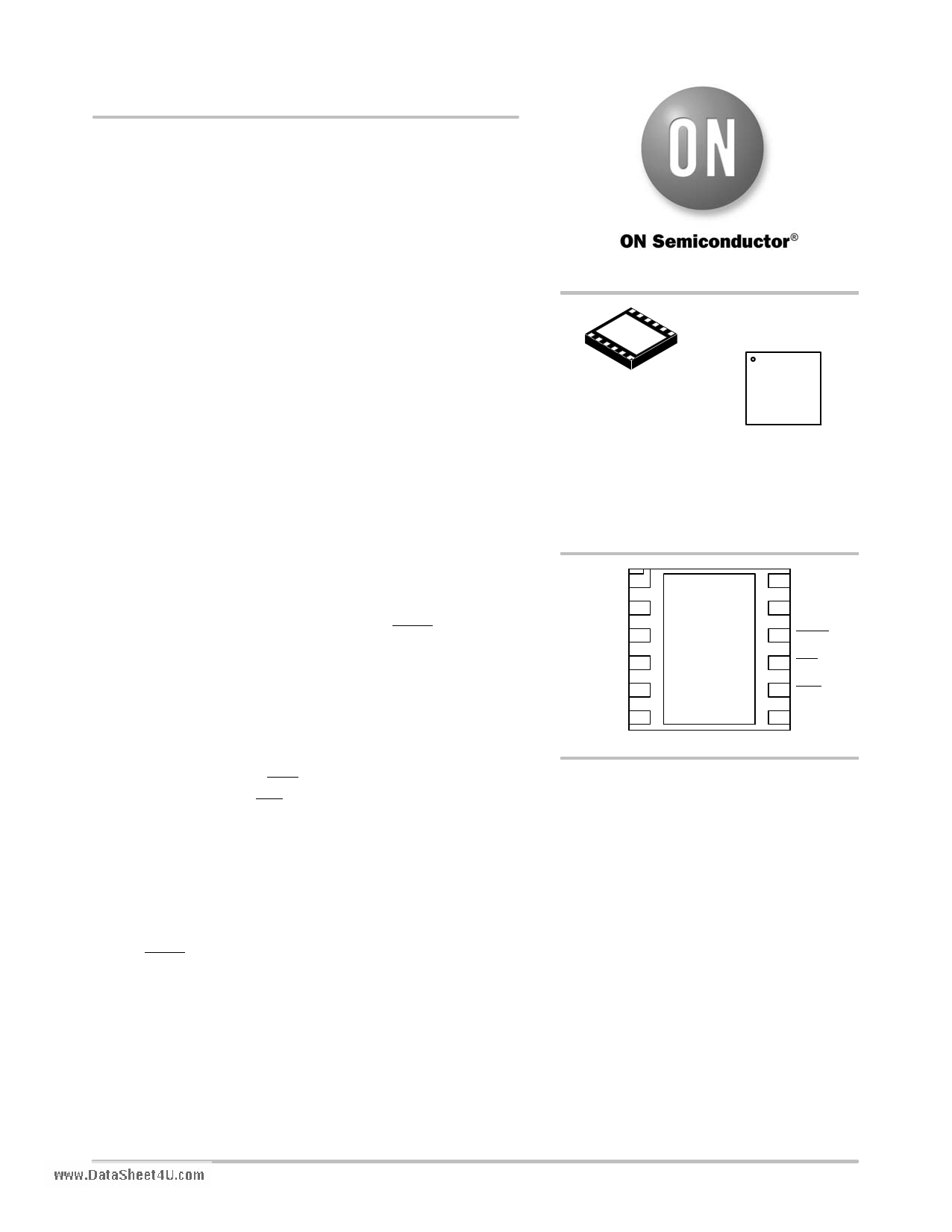
MARKING
DIAGRAM
1
12 PIN LLGA
MU SUFFIX
CASE 513AK
NCAI
370
ALYWG
G
A = Assembly Location
L = Wafer Lot
Y = Year
W = Work Week
G = Pb−Free Package
(Note: Microdot may be in either location)
IN 1
IN 2
GND 3
RES 4
RES 5
NCP370
12 NC
11 OUT
10 FLAG
9 DIR
8 REV
Features
• Overvoltage Protection Up to 28 V
• Negative Voltage Protection Down to −28 V
• Reverse Charge Control: REV
• Direct Charge Control: DIR
• Overcurrent Protection
• Thermal Shutdown
• On−chip Low RDS(on) NMOS Transistors: Typical 130 mW
• Overvoltage Lockout (OVLO)
• Undervoltage Lockout (UVLO)
• Soft−Start
• Alert FLAG Output
• Compliance to IEC61000−4−2 (Level 4)
8 kV (Contact)
15 kV (Air)
• ESD Ratings: Machine Model = B
Human Body Model = 2
• 12 Lead TLLGA 3x3 mm Package
• This is a Pb−Free Device
RES 6
(Top View)
7 Ilim
ORDERING INFORMATION
See detailed ordering and shipping information in the package
dimensions section on page 10 of this data sheet.
Typical Applications
• Cell Phones
• Camera Phones
• Digital Still Cameras
• Personal Digital Applications
• MP3 Players
© Semiconductor Components Industries, LLC, 2008
December, 2008 − Rev. 2
1
Publication Order Number:
NCP370/D
1 page 
NCP370
Characteristics
Symbols
Conditions
TIMINGS
DIRECT MODE
Start Up Delay
FLAG Going Up Delay
Turn Off Delay
Alert Delay
Disable Time
ton From Vin > UVLO to Vout w 0.3 V
tstart
From Vout > 0.3 V to FLAG = 1.2 V
toff From Vin > OVLO to Vout v 0.3 V
Vin Increasing from 5 V to 8 V at 3 V/ms
tstop From Vin > OVLO to FLAG v 0.4 V See Figure
3 and 9 Vin Increasing from 5 V to 8 V at 3 V/ms
tdis
REV
=
1.2
V,
From
DIR =
v 0.3
0.4
V
V
to
1.2
V
to
Vout
REVERSE MODE
Reverse Start Up Delay
tonREV
Vout
w 2.5 V, From REV = 1.2 to 0.55
Vin w 0.3 V, Reverse Mode
to
Reverse FLAG Going Up Delay
tstartREV
From Vin w 0.3 V FLAG = 1.2 V, Reverse Mode
Rearming Reverse Delay
tRRD
Vout > 2.5 V, Rin = 1 W, Reverse Mode
Over Current Regulation Time
tREG
Vout > 2.6, Vin > 0.3 V, Reverse Mode
OCP Delay Time
tOCP
From Ireverse > Ilim, 1 A/1 ms
Reverse Disable Time
tREVDIS
From REV = 0.55 V to 1.2 V, to Vin < 0.3 V.
Vout = 5 V
NOTE: Electrical parameters are guaranteed by correlation across the full range of temperature.
Min wwTywp.DataMSahxeet4UUn.citom
20 30 40 ms
20 30 40 ms
1.5 5.0 ms
1.5 ms
2.5 ms
0.6 1.2 1.8 ms
0.6 1.2 1.8 ms
20 30 40 ms
0.5 1.2 1.8 ms
5 ms
200 ms
TYPICAL OPERATING CHARACTERISTICS
Operation
The NCP370 provides overvoltage protection for positive
and negative voltages, up to 28 V or down to −28 V on
IN pins. At powerup, with DIR pin = low, REV = high, the
output rises 30 ms after the input rises above the UVLO. The
NCP370 provides a FLAG output, which alerts the system
that a fault has occurred. The FLAG signal rises 30 ms after
the output signal rises.
A Reverse Mode is available when an accessory is
connected on IN pins and the internal battery is applied on
the OUT pin, allowing the accessory to be powered. In this
mode, no supply must be connected on IN pins and REV pin
must be tied to low level. The NCP370 provides overcurrent
protection for the battery from current faults in the
accessory.
Undervoltage Lockout (UVLO)
To ensure proper turn−on operation from AC/DC (or Wall
adapter charging) under any conditions, the device has a
built−in undervoltage lock out (UVLO) circuit. During
positive going slope on Vin, the output remains disconnected
from input until Vin voltage is above UVLO. The FLAG
output will be low as long as Vin has not reached UVLO
threshold. This circuit has a 60 mV hysteresis to provide
noise immunity to transient conditions.
In Reverse Mode (REV pin v 0.55 V, DIR w 1.2 V),
UVLO and OVLO comparators are inactivated.
Overvoltage Lockout (OVLO)
To protect connected systems on Vout pin from
overvoltage, the device has a built−in overvoltage lock out
(OVLO) circuit. During overvoltage condition, the output is
disabled as long as the input voltage exceeds OVLO.
Additional OVLO thresholds can be manufactured
(Please contact your ON Semiconductor representative for
availability).
FLAG output will be low since Vin is higher than OVLO.
This circuit has a 80 mV hysteresis to provide noise
immunity to transient conditions.
Oversystem Voltage Lockout (OVLO00)
A second overvoltage comparator is available for
supplying the sytem (output) by the Wall Adaptor (input) by
setting DIR = low and REV = low. The RDS(on) will be
higher during this mode allowing to handle few 10 mA.
This additional comparator allows to put higher input
voltage (OVLO = 8.27 V typical) on the NCP370 during test
production sequence (I.E: One Time Programming of the
cell phone, PDA). This parameter is 25°C guaranteed only.
FLAG Output
The NCP370 provides a FLAG output which alerts that a
fault has occurred. As soon as a fault state is detected by the
NCP370 (see Figure 3), the FLAG pin output goes low,
alerting the micro−controller to take appropriate action.
http://onsemi.com
5
5 Page 
NCP370
PACKAGE DIMENSIONS
www.DataSheet4U.com
D
PIN ONE
REFERENCE
ÇÇÇ2X
ÇÇÇ0.15 C
ÇÇÇ2X
0.15 C
TOP VIEW
0.10 C
12X 0.08 C
A1
SIDE VIEW
D2
16
12X K
AB
LLGA12 3x3, 0.5P
CASE 513AK−01
ISSUE O
E
A
C
SEATING
PLANE
NOTES:
1. DIMENSIONING AND TOLERANCING PER
ASME Y14.5M, 1994.
2. CONTROLLING DIMENSION: MILLIMETERS.
3. DIMENSION b APPLIES TO PLATED
TERMINAL AND IS MEASURED BETWEEN
0.15 AND 0.30 MM FROM TERMINAL TIP.
4. COPLANARITY APPLIES TO THE EXPOSED
PAD AS WELL AS THE TERMINALS.
MILLIMETERS
DIM MIN MAX
A 0.50 0.60
A1 0.00 0.05
b 0.20 0.30
D 3.00 BSC
D2 2.60 2.80
E 3.00 BSC
E2 1.90 2.10
e 0.50 BSC
K 0.20 −−−
L 0.25 0.35
SOLDERING FOOTPRINT*
3.30
1
12X
0.50
e 0.43
E2
0.50
PITCH
2.75
12X L
12 7
BOTTOM VIEW
12X
b
0.10 C A B
0.05 C NOTE 3
11X
0.30
2.05
DIMENSIONS: MILLIMETERS
*For additional information on our Pb−Free strategy and soldering
details, please download the ON Semiconductor Soldering and
Mounting Techniques Reference Manual, SOLDERRM/D.
The products described herein (NCP370), may be covered by one or more U.S. patents. There may be other patents pending.
ON Semiconductor and
are registered trademarks of Semiconductor Components Industries, LLC (SCILLC). SCILLC reserves the right to make changes without further notice
to any products herein. SCILLC makes no warranty, representation or guarantee regarding the suitability of its products for any particular purpose, nor does SCILLC assume any liability
arising out of the application or use of any product or circuit, and specifically disclaims any and all liability, including without limitation special, consequential or incidental damages.
“Typical” parameters which may be provided in SCILLC data sheets and/or specifications can and do vary in different applications and actual performance may vary over time. All
operating parameters, including “Typicals” must be validated for each customer application by customer’s technical experts. SCILLC does not convey any license under its patent rights
nor the rights of others. SCILLC products are not designed, intended, or authorized for use as components in systems intended for surgical implant into the body, or other applications
intended to support or sustain life, or for any other application in which the failure of the SCILLC product could create a situation where personal injury or death may occur. Should
Buyer purchase or use SCILLC products for any such unintended or unauthorized application, Buyer shall indemnify and hold SCILLC and its officers, employees, subsidiaries, affiliates,
and distributors harmless against all claims, costs, damages, and expenses, and reasonable attorney fees arising out of, directly or indirectly, any claim of personal injury or death
associated with such unintended or unauthorized use, even if such claim alleges that SCILLC was negligent regarding the design or manufacture of the part. SCILLC is an Equal
Opportunity/Affirmative Action Employer. This literature is subject to all applicable copyright laws and is not for resale in any manner.
PUBLICATION ORDERING INFORMATION
LITERATURE FULFILLMENT:
Literature Distribution Center for ON Semiconductor
P.O. Box 5163, Denver, Colorado 80217 USA
Phone: 303−675−2175 or 800−344−3860 Toll Free USA/Canada
Fax: 303−675−2176 or 800−344−3867 Toll Free USA/Canada
Email: [email protected]
N. American Technical Support: 800−282−9855 Toll Free
USA/Canada
Europe, Middle East and Africa Technical Support:
Phone: 421 33 790 2910
Japan Customer Focus Center
Phone: 81−3−5773−3850
http://onsemi.com
11
ON Semiconductor Website: www.onsemi.com
Order Literature: http://www.onsemi.com/orderlit
For additional information, please contact your local
Sales Representative
NCP370/D
11 Page | ||
| Páginas | Total 11 Páginas | |
| PDF Descargar | [ Datasheet NCP370.PDF ] | |
Hoja de datos destacado
| Número de pieza | Descripción | Fabricantes |
| NCP370 | Positive and Negative Overvoltage Protection | ON Semiconductor |
| NCP370 | Positive and Negative Overvoltage Protection | ON Semiconductor |
| NCP3712ASNT1 | Over Voltage Protected High Side Switch | ON Semiconductor |
| NCP372 | Positive and Negative Overvoltage Protection Controller | ON Semiconductor |
| Número de pieza | Descripción | Fabricantes |
| SLA6805M | High Voltage 3 phase Motor Driver IC. |
Sanken |
| SDC1742 | 12- and 14-Bit Hybrid Synchro / Resolver-to-Digital Converters. |
Analog Devices |
|
DataSheet.es es una pagina web que funciona como un repositorio de manuales o hoja de datos de muchos de los productos más populares, |
| DataSheet.es | 2020 | Privacy Policy | Contacto | Buscar |