|
|
|
PDF SCAN90CP02 Data sheet ( Hoja de datos )
| Número de pieza | SCAN90CP02 | |
| Descripción | 1.5 Gbps 2x2 LVDS Crosspoint Switch | |
| Fabricantes | National Semiconductor | |
| Logotipo | ||
Hay una vista previa y un enlace de descarga de SCAN90CP02 (archivo pdf) en la parte inferior de esta página. Total 16 Páginas | ||
|
No Preview Available !
May 2007
SCAN90CP02
1.5 Gbps 2x2 LVDS Crosspoint Switch with Pre-Emphasis
and IEEE 1149.6
General Description
The SCAN90CP02 is a 1.5 Gbps 2 x 2 LVDS crosspoint
switch. High speed data paths and flow-through pinout mini-
mize internal device jitter, while configurable 0/25/50/100%
pre-emphasis overcomes external ISI jitter effects of lossy
backplanes and cables. The differential inputs interface to
LVDS and Bus LVDS signals such as those on National's 10-,
16-, and 18- bit Bus LVDS SerDes, as well as CML and
LVPECL. The SCAN90CP02 can also be used with ASICs
and FPGAs. The non-blocking crosspoint architecture is pin-
configurable as a 1:2 clock or data splitter, 2:1 redundancy
mux, crossover function, or dual buffer for signal booster and
stub hider applications.
Integrated IEEE 1149.1 (JTAG) and 1149.6 circuitry supports
testability of both single-ended LVTTL/CMOS and differential
LVDS PCB interconnect. The 3.3V supply, CMOS process,
and LVDS I/O ensure high performance at low power over the
entire industrial -40 to +85°C temperature range.
Features
■ 1.5 Gbps per channel
■ Low power: 70 mA in dual repeater mode @1.5 Gbps
■ Low output jitter
■ Configurable 0/25/50/100% pre-emphasis drives lossy
backplanes and cables
■ Non-blocking architecture allows 1:2 splitter, 2:1 mux,
crossover, and dual buffer configurations
■ Flow-through pinout
■ LVDS/BLVDS/CML/LVPECL inputs, LVDS Outputs
■ IEEE 1149.1 and 1149.6 compliant
■ Single 3.3V supply
■ Separate control of inputs and outputs allows for power
savings
■ Industrial -40 to +85°C temperature range
■ 28-lead LLP package, or 32-lead LQFP package
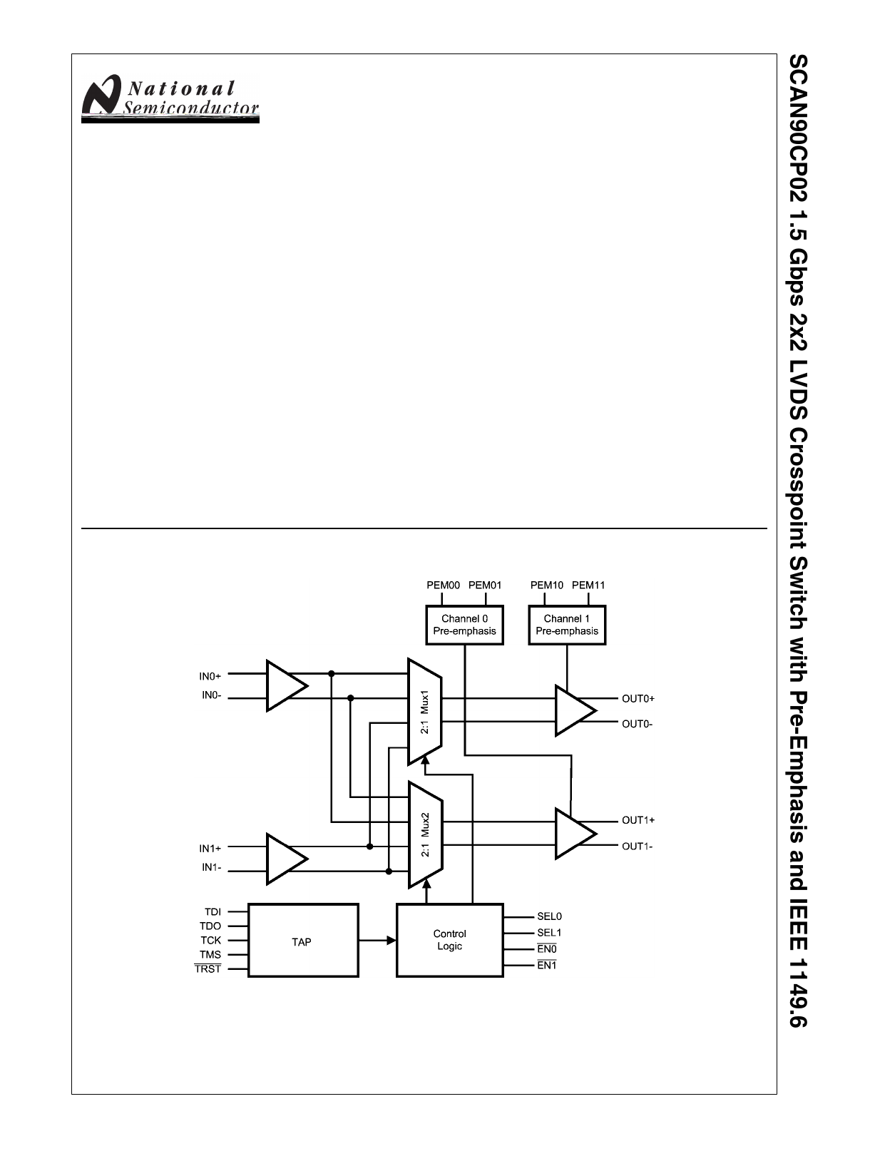
Block Diagram
FIGURE 1. SCAN90CP02 Block Diagram
20071401
© 2007 National Semiconductor Corporation 200714
www.national.com
1 page 
Absolute Maximum Ratings (Note 3)
If Military/Aerospace specified devices are required,
please contact the National Semiconductor Sales Office/
Distributors for availability and specifications.
Supply Voltage (VDD)
CMOS Input Voltage
LVDS Receiver Input Voltage
−0.3V to +4.0V
−0.3V to (VDD +0.3V)
−0.3V to +3.6V
LVDS Driver Output Voltage
−0.3V to +3.6V
LVDS Output Short Circuit Current
40mA
Junction Temperature
+150°C
Storage Temperature
−65°C to +150°C
Lead Temperature
(Soldering, 4sec.)
+260°C
Maximum Package Power Dissipation at 25°C
LLP-28
4.31 W
LQFP-32
1.47 W
Derating above 25°C
LLP-28
34.5 mW/°C
LQFP-32
Thermal Resistance, θJA
LLP-28
LQFP-32
ESD Rating
HBM, 1.5 kΩ, 100 pF
EIAJ, 0Ω, 200 pF
11.8 mW/°C
29°C/W
85°C/W
6.5 kV
>250V
Recommended Operating
Conditions
Supply Voltage (VDD– GND)
Receiver Input Voltage
Operating Free Air
Temperature
Junction Temperature
Min Typ Max Unit
3.0 3.3 3.6 V
0 3.6 V
−40 25 85 °C
150 °C
Electrical Characteristics
Over recommended operating supply and temperature ranges unless other specified.
Symbol
Parameter
Conditions
Min
Typ
(Note 4)
Max
LVTTL DC SPECIFICATIONS (SEL0, SEL1, EN1, EN2, PEM00, PEM01, PEM10, PEM11, TDI, TCK, TMS, TRST)
VIH High Level Input Voltage
VIL Low Level Input Voltage
IIH High Level Input Current
VIN = VDD = VDDMAX
IIL Low Level Input Current
VIN = VSS, VDD = VDDMAX
IILR Low Level Input Current
TDI, TMS, TRST
CIN1 Input Capacitance
Any Digital Input Pin to VSS
COUT1 Output Capacitance
Any Digital Output Pin to VSS
VCL Input Clamp Voltage
ICL = −18 mA
VOH High Level Output Voltage
(TDO)
IOH = −12 mA, VDD = 3.0 V
IOH = −100 µA, VDD = 3.0 V
VOL Low Level Output Voltage
(TDO)
IOL = 12 mA, VDD = 3.0 V
IOL = 100 µA, VDD = 3.0 V
IOS Output Short Circuit Current
TDO
LVDS INPUT DC SPECIFICATIONS (IN0±, IN1±)
2.0
GND
−10
−10
-40
−1.5
2.4
VDD-0.2
3.5
5.5
−0.8
-15
VDD
0.8
+10
+10
-200
0.5
0.2
-125
VTH Differential Input High Threshold VCM = 0.8V or 1.2V or 3.55V, VDD = 3.6V
(Note 5)
0 100
VTL Differential Input Low Threshold VCM = 0.8V or 1.2V or 3.55V, VDD = 3.6V −100
0
VID Differential Input Voltage
VCM = 0.8V to 3.55V, VDD = 3.6V
100
VCMR
Common Mode Voltage Range
VID = 150 mV, VDD = 3.6V
0.05
3.55
CIN2 Input Capacitance
IN+ or IN− to VSS
3.5
IIN Input Current
VIN = 3.6V, VDD = VDDMAX or 0V
−10
+10
VIN = 0V, VDD = VDDMAX or 0V
−10
+10
Units
V
V
µA
µA
µA
pF
pF
V
V
V
V
V
mA
mV
mV
mV
V
pF
µA
µA
5 www.national.com
5 Page 
Typical Performance Characteristics for LLP Package
Power Supply Current vs. Bit Data Rate
Total Jitter (TJ) vs. Bit Data Rate
20071441
20071442
Dynamic power supply current was measured while running a PRBS 223-1 patternTotal Jitter measured at 0V differential while running a PRBS 223-1 pattern in
in dual channel repeater mode. VCC = 3.3V, TA = +25°C, VID = 0.5V, VCM = 1.2Vsingle channel repeater mode. VCC = 3.3V, TA = +25°C, VID = 0.5V, 0% Pre-
emphasis
Total Jitter (TJ) vs. Temperature
Positive Edge Transition vs. Pre-emphasis Level
20071443
Total Jitter measured at 0V differential while running a PRBS 223-1 pattern in dual
channel repeater mode. VCC = 3.3V, VID = 0.5V, VCM = 1.2V, 1.5 Gbps data rate,
0% Pre-emphasis
FIGURE 7. Typical Performance Characteristics
20071455
11 www.national.com
11 Page | ||
| Páginas | Total 16 Páginas | |
| PDF Descargar | [ Datasheet SCAN90CP02.PDF ] | |
Hoja de datos destacado
| Número de pieza | Descripción | Fabricantes |
| SCAN90CP02 | SCAN90CP02 1.5 Gbps 2x2 LVDS Crosspoint Switch w/Pre-Emphasis IEEE 1149.6 (Rev. M) | Texas Instruments |
| SCAN90CP02 | 1.5 Gbps 2x2 LVDS Crosspoint Switch | National Semiconductor |
| Número de pieza | Descripción | Fabricantes |
| SLA6805M | High Voltage 3 phase Motor Driver IC. |
Sanken |
| SDC1742 | 12- and 14-Bit Hybrid Synchro / Resolver-to-Digital Converters. |
Analog Devices |
|
DataSheet.es es una pagina web que funciona como un repositorio de manuales o hoja de datos de muchos de los productos más populares, |
| DataSheet.es | 2020 | Privacy Policy | Contacto | Buscar |