|
|
PDF NLAST4053 Data sheet ( Hoja de datos )
| Número de pieza | NLAST4053 | |
| Descripción | Analog Multiplexer/ Demultiplexer | |
| Fabricantes | ON Semiconductor | |
| Logotipo | ||
Hay una vista previa y un enlace de descarga de NLAST4053 (archivo pdf) en la parte inferior de esta página. Total 14 Páginas | ||
|
No Preview Available !
NLAST4053
www.DataSheet4U.com
Analog Multiplexer/
Demultiplexer
TTL Compatible, Triple 2:1 Analog
Switch-Multiplexer Improved Process,
Sub-Micron Silicon Gate CMOS
The NLAST4053 is an improved version of the MC14053 and
MC74HC4053 fabricated in sub-micron Silicon Gate CMOS
technology for lower RDS(on) resistance and improved linearity with
low current. This device may be operated either with a single supply or
dual supply up to ±3 V to pass a 6 VPP signal without coupling
capacitors.
When operating in single supply mode, it is only necessary to tie
VEE, pin 7 to ground. For dual supply operation, VEE is tied to a
negative voltage, not to exceed maximum ratings. Translation is
provided in the device, the Address and Inhibit pins are standard TTL
level compatible. For CMOS compatibility see NLAS4053. Pin for
pin compatible with all industry standard versions of `4053.'
•ăImproved RDS(on) Specifications
•ăPin for Pin Replacement for MAX4053 and MAX4053A
- One Half the Resistance Operating at 5.0 Volts
•ăSingle or Dual Supply Operation
- Single 3-5 Volt Operation, or Dual ±3 Volt Operation
- With VCC of 3.0 to 3.3 V, Device Can Interface with 1.8 V Logic,
- No Translators Needed
- Address and Inhibit Pins are Over-Voltage Tolerant and May Be
- Driven Up +6ĂV Regardless of VCC
•ăAddress and Inhibit Pins are Standard TTL Compatible
- Greatly Improved Noise Margin Over MAX4053 and MAX4053A
- True TTL Compatibility VIL = 0.8 V, VIH = 2.0 V
•ăImproved Linearity Over Standard HC4053 Devices
•ăPopular SOIC, and Space Saving TSSOP, and QSOP 16 Pin
Packages
•ăThis is a Pb-Free Device
http://onsemi.com
MARKING
DIAGRAM
TSSOP-16
DT SUFFIX
CASE 948F
16
AST
4053
ALYW
1
A = Assembly Location
L = Wafer Lot
Y = Year
W = Work Week
ORDERING INFORMATION
Device
Package
Shipping†
NLAST4053DTR2G TSSOP-16 2500 / Tape &
(Pb-Free)
Reel
†For information on tape and reel specifications,
including part orientation and tape sizes, please
refer to our Tape and Reel Packaging Specifications
Brochure, BRD8011/D.
©Ă Semiconductor Components Industries, LLC, 2008
February, 2008 - Rev. 1
1
Publication Order Number:
NLAST4053/D
1 page 
NLAST4053
AC CHARACTERISTICS (Input tr = tf = 3 ns)
ÎÎÎÎÎÎÎÎÎÎÎÎÎÎÎÎÎÎÎÎÎÎÎÎÎÎÎÎÎÎÎÎÎÎÎÎÎÎÎÎÎÎÎÎÎÎÎÎÎÎÎÎÎÎÎÎÎÎÎÎÎÎÎÎÎÎÎÎÎÎÎÎÎÎÎÎÎÎÎÎÎÎÎÎÎÎÎÎÎÎÎÎÎÎÎÎÎÎÎSymbol
Parameter
Test Conditions
ÎÎÎÎÎÎÎÎÎÎÎÎÎÎÎÎÎÎÎÎÎÎÎÎÎÎÎÎÎÎÎÎÎtBBM
Minimum Break-Before-Make VIN = VIL or VIH
www.DataSheet4U.com
Guaranteed Limit
VCC
V
3.0
VEE
V
0.0
-55 to 25°C
Min Typ*
1.0 6.5
v85°C v125°C Unit
- - ns
Time
VIS = VCC
4.5 0.0 1.0
5.0
-
-
RL = 300 W, CL = 35 pF
3.0 -3.0 1.0
3.5
-
-
(Figure 19)
*Typical Characteristics are at 25°C.
AC CHARACTERISTICS (CL = 50 pF, Input tr = tf = 3 ns)
Guaranteed Limit
Symbol
Parameter
VCC
V
VEE
V
-55 to 25°C
Min Typ Max
v85°C
Min Max
v125°C
Min Max
Unit
tTRANS
Transition Time
(Address Selection Time)
(Figure 18)
2.5 0
3.0 0
4.5 0
3.0 -3.0
40 45 50 ns
28 30 35
23 25 30
23 25 28
tON Turn-on Time
2.5 0
(Figures 14, 15, 20, and 21)
3.0 0
Enable to NO or NC
4.5 0
3.0 -3.0
40 45 50 ns
28 30 35
23 25 30
23 25 28
tOFF
Turn-off Time
(Figures 14, 15, 20, and 21)
Enable to NO or NC
2.5 0
3.0 0
4.5 0
3.0 -3.0
40 45 50 ns
28 30 35
23 25 30
23 25 28
CIN
CNO or CNC
CCOM
C(ON)
Maximum Input Capacitance,Select Inputs
Analog I/O
Common I/O
Feedthrough
Typical @ 25°C, VCC = 5.0 V
8
10
10
1.0
pF
http://onsemi.com
5
5 Page 
Open
Input
NLAST4053
DUT
VCC
Output
300 W
VOUT
35 pF
Enable
VCC
Input
0V
Output
VOL
50%
VCC
10%
tOFF
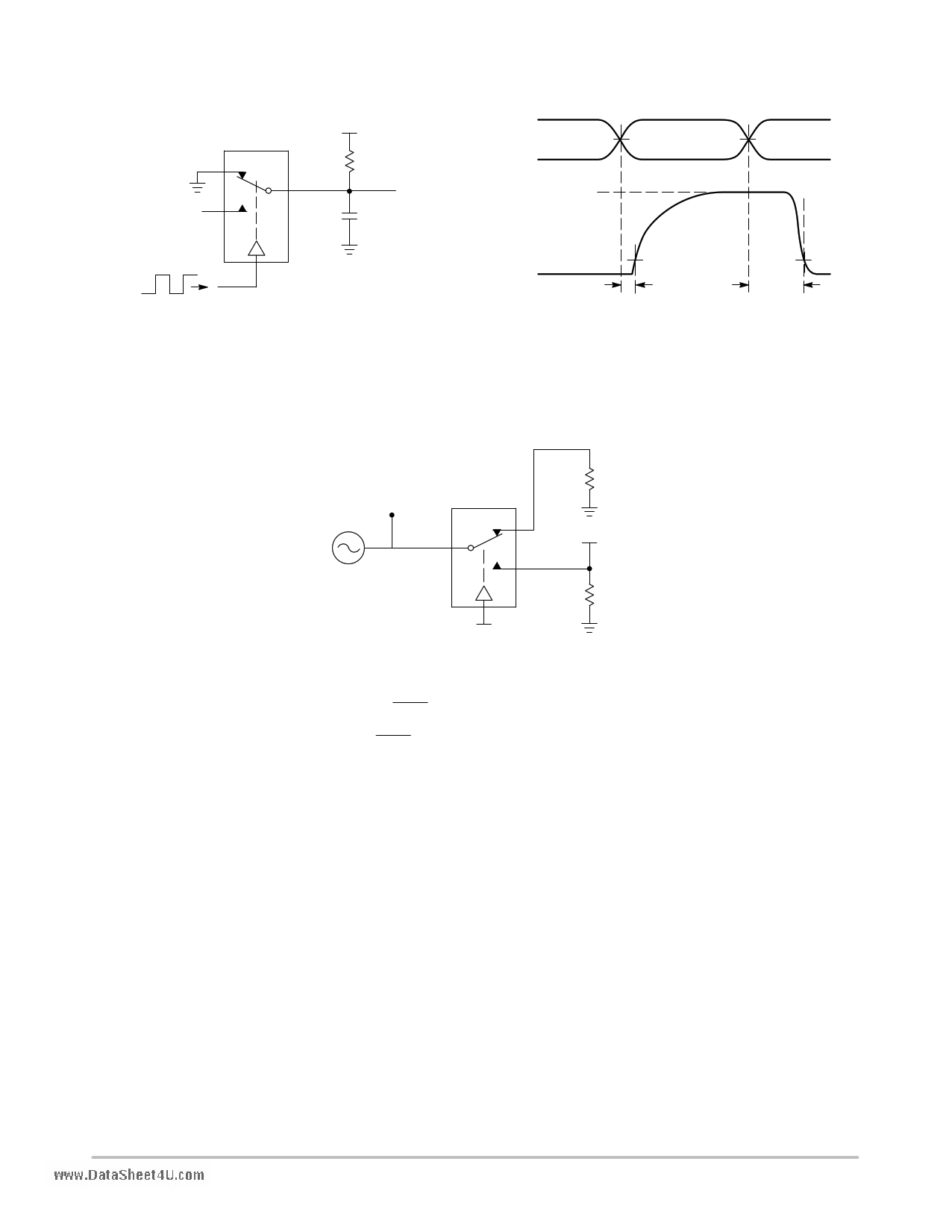
Figure 21. tON/tOFF
www.DataSheet4U.com
50%
10%
tON
Reference
DUT
Input
50 W Generator
Output
50 W
Transmitted
50 W
Channel switch control/s test socket is normalized. Off isolation is measured across an off channel. On loss is
the bandwidth of an On switch. VISO, Bandwidth and VONL are independent of the input signal direction.
ǒ ǓVOUT
VISO = Off Channel Isolation = 20 Log VIN for VIN at 100 kHz
ǒ ǓVONL = On Channel Loss = 20 Log
VOUT
VIN
for VIN at 100 kHz to 50 MHz
Bandwidth (BW) = the frequency 3 dB below VONL
Figure 22. Off Channel Isolation/On Channel Loss (BW)/Crosstalk
(On Channel to Off Channel)/VONL
http://onsemi.com
11
11 Page | ||
| Páginas | Total 14 Páginas | |
| PDF Descargar | [ Datasheet NLAST4053.PDF ] | |
Hoja de datos destacado
| Número de pieza | Descripción | Fabricantes |
| NLAST4051 | Analog Multiplexer / Demultiplexer | ON |
| NLAST4052 | Analog Multiplexer/Demultiplexer | ON Semiconductor |
| NLAST4053 | Analog Multiplexer/ Demultiplexer | ON Semiconductor |
| Número de pieza | Descripción | Fabricantes |
| SLA6805M | High Voltage 3 phase Motor Driver IC. |
Sanken |
| SDC1742 | 12- and 14-Bit Hybrid Synchro / Resolver-to-Digital Converters. |
Analog Devices |
|
DataSheet.es es una pagina web que funciona como un repositorio de manuales o hoja de datos de muchos de los productos más populares, |
| DataSheet.es | 2020 | Privacy Policy | Contacto | Buscar |
