|
|
|
PDF SC2616 Data sheet ( Hoja de datos )
| Número de pieza | SC2616 | |
| Descripción | Complete DDR Power Solution | |
| Fabricantes | Semtech | |
| Logotipo | ||
Hay una vista previa y un enlace de descarga de SC2616 (archivo pdf) en la parte inferior de esta página. Total 17 Páginas | ||
|
No Preview Available !
POWER MANAGEMENT
Description
The SC2616 is a fully integrated DDR power solution pro-
viding power for the VDDQ and the VTT rails. The SC2616
also completely adheres to the ACPI sleep state power
requirements. A synchronous buck controller provides
the high current of the VDDQ at high efficiency, while a
linear sink/source regulator provides the termination
voltage with 2 Amp Source/Sink capability. This approach
makes the best trade-off between cost and perfor-
mance. Additional logic and UVLOs complete the func-
tionality of this single chip DDR power solution in compli-
ance with S3 and S5 motherboard signals.
The SC2616 is capable of sourcing up to 20A at the
switcher output, and 2A source/sink at the VTT output.
The MLP package provides excellent thermal impedance
while keeping small footprint. VDDQ current limit as well
as 3 independent thermal shutdown circuits assure safe
operation under all fault conditions.
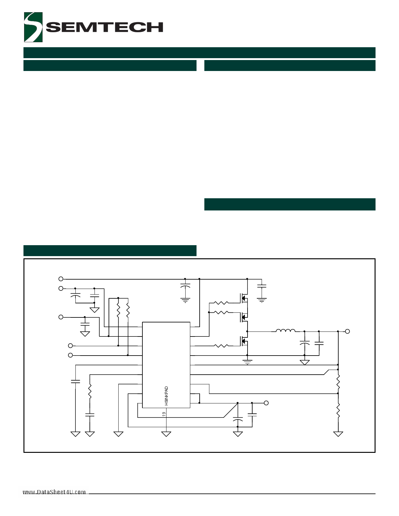
Typical Application Circuit
SC2616
Complete DDR Power Solution
www.DataSheet4U.com
Features
High efficiency (90%) switcher for VDDQ supplies
20 Amps
High current gate drives
Single chip solution complies fully with ACPI power
sequencing specifications
Internal S3 state LDO supplies high standby
VDDQ current (0.65Amp Min.)
ACPI sleep state controlled
2 Amp VTT source/sink capability
UVLO on 5V and 12V
Independent thermal shutdown for VDDQ and VTT
Fast transient response
18 pin MLP package
Applications
Power solution for DDR memory per ACPI
motherboard specification
High speed data line termination
Memory cards
5V
12V
10uF 0.1uF
5V STBY
0.1uF
Suspend to RAM
Suspend to disk
0.1uF
C in
10k 10k
S3
S5
U4 SC2616
16 12VCC
5VCC
4 5VSBY
TG
11 SLP_S3
BG
10 SLP_S5
PGND
18 SS/EN
VDDQSTBY
17 COMP
VDDQIN
12 AGND
FB
3 LGND
VTT
2 VTTSNS
VTT
9
15
14
13
7
8
1
6
5
1uF
L
C out
0.1uF
VDDQ
VTT
0.1uF
Revision 3, March 2003
1
www.semtech.com
1 page 
SC2616
POWER MANAGEMENT
Pin Configuration
TOP VIEW
FB
VTTSNS
LGND
5VSBY
VTT
VTT
VDDQSTBY
VDDQIN
5VCC
1
2
3
4
5
6
7
8
9
18 SS/EN
17 COMP
16 12VCC
15 TG
14 BG
13 PGND
12 AGND
11 SLP_S3
10 SLP_S5
www.DataSheet4U.com
Ordering Information
Part Numbers
Package
SC2616MLTR(1)
MLP-18
Note:
(1) Only available in tape and reel packaging. A reel
contains 3000 devices.
(18 Pin MLP)
Note: Pin 19 is the thermal Pad on the bottom
of the device
Pin Descriptions
Pin # Pin Name
Pin Function
1 FB Feedback for the STBY LDO and the switcher for VDDQ.
2 VTTSNS VTT LDO feedback and remote sense input.
3 LGND VTT return. Connect to point of load return. The trace connecting to this pin must be able to carry
2 Amps.
4 5VSBY Bias supply for the chip. Connect to 5V standby.
5, 6 VTT VTT return. Connect to point of load return. The trace connecting to this pin must be able to carry
2 Amps.
7 VDDQSTBY S3 VDDQ output. Provision must be made to prevent the VDDQSTBY supply from back feeding
the input supply (see typical application schematic). Traces connecting to this pin must be
capable of carring 1 Amp.
8 VDDQIN VDDQ power input to VTT LDO. The trace connecting to this pin must be able to carry 2 Amps.
9 5VCC Supply to the lower gate drive.
10 SLP_S5 Connect to S5 signal from motherboard.
11 SLP_S3 Connect to S3 signal from motherboard.
12 AGND Analog ground.
13 PGND Gate drive return. Keep this pin close to bottom FET source.
14 BG Bottom gate drive.
15 TG Top gate drive.
16 12VCC Supply to the upper and lower gate drives.
17 COMP Compensation pin for the PWM transconductance amplifier.
18 SS/EN Soft start capacitor to GND. Pull low to less than 0.3V to disable controller.
19 TH_PAD
2003 Semtech Corp.
Copper pad on bottom of chip used for heatsinking. This pin is internally connected to AGND.
5 www.semtech.com
5 Page 
SC2616
POWER MANAGEMENT
Applications Information
Description
The Semtech SC2616 DDR power supply controller is
the latest and most complete switching and linear
regulator combination, providing the necessary functions
to comply with S3 and S5 sleep state signals generated
by the Desktop Computer Motherboards. VDDQ supply,
and VTT termination voltage are supplied to the Memory
bus during S0 (normal operation) state. During S0, VDDQ
is supplied via the Switching regulator, sourcing high
output currents to the VDD bus as well as supplying the
termination supply current. The SC2616 is capable of
driving a 4000pf capacitor in 25ns (typical, top gate).
This drive capability allows 15-20A DC load on the VDDQ
supply. The VTT termination voltage is an internal sink/
source linear regulator, which during S0 state receives
its power from the VDDQ bus. It is capable of sourcing
and sinking 2 Amps (max). The current limit on this pin is
set to 3 Amps (typical).
Output Current and PCB layout
The current handling capacity of SC2616 depends upon
the amount of heat the PC board can sink from the
SC2616 thermal pad. (See mounting instructions). The
PC board layout must take into consideration the high
current paths, and ground returns for both the VDDQ
and VTT supply pins. VTT, LGND, VDDQ, 5VCC and PGND
traces must also be routed using wide traces to minimize
power loss and heat in these traces, based on the current
handling requirements.
S3 and S5 States
During S3 and S5 sleep states, the operation of the VDDQ
and VTT supplies is governed by the internal sequencing
logic in strict adherence with motherboard specifications.
The timing diagram demonstrates the state of the
controller, and each of the VDDQ and VTT supplies during
S3 and S5 transitions. When S3 is low, the VDDQ supplies
the “Suspend To RAM” current of 650 mA (min) to
maintain the information in memory while in standby
mode. The VTT termination voltage is not needed during
this state, and is thus tri-stated during S3. Once S3 goes
high, the VDDQ switcher recovers and takes control of
the VDDQ supply voltage. When S5 and S3 are pulled
low, all supplies shut down. The SS/EN pin must be pulled
low (<0.3V) and high again to restart the SC2616. This
can be achieved by cycling the input supplies, 5V and
www.DataSheet4U.com
12V since both supplies have to be higher than their UVLO
thresholds for proper start-up.
Initial Conditions and Event Sequencing
The main switcher will start-up in Asynchronous Mode
when the voltage on SS/EN pin is greater than ~0.3V.
The SS/EN will go high only after the 5Vcc and 12Vcc are
higher than their respective UVLO thresholds. The switcher
achieves maximum duty cycle when SS/EN reaches 0.8V.
When the SS/EN equals 1.25V, the synchronous FET will
also be activated.
When the S5 and S3 go high for the first time, the VDDQ
is supplied by the switcher, thus removing the burden of
charging the output capacitors via the linear regulator.
An internal latch guarantees that the supply goes through
S0 state for the first time.
During a transition from S3 to S0, where the 5V and 12V
rails and subsequently the SS/EN pin go high, the internal
VDDQ standby supply will remain ”on” until SS/EN has
reached 1V, at which point only the switcher is supplying
VDDQ , andthe internal “power good” indicator goes high.
The “Memory” activity should be slaved off the “Power
OK” signal from the Silver Box supply, and since the “Power
OK” is asserted after all supplies are within close tolerance
of their final values, the VDDQ switcher should have
been running for some time before the memory is
activated. This is true for typical SS/EN capacitor values
(10nf to 220nf). Thus during transitions from S3 to S0,
the concern that the VDDQ Standby supply may have to
provide high currents before the switcher is activated is
alleviated.
The logic inputs to S3 and S5 pins must be defined before
application of power to the SC2616. This can be
guaranteed by pulling up the S3 and S5 inputs to
5VStandby. If the chipset that asserts these signals is
powered after the SC2616 powers up, and S3 and S5
are not pulled up, erroneous startup and operation can
result.
Care must be taken not to exceed the maximum voltage/
current specifications on to the interface supplying these
signals. The pullup voltage and resistor must be chosen
such that when high, the S3 and S5 do not “back drive”
2003 Semtech Corp.
11
www.semtech.com
11 Page | ||
| Páginas | Total 17 Páginas | |
| PDF Descargar | [ Datasheet SC2616.PDF ] | |
Hoja de datos destacado
| Número de pieza | Descripción | Fabricantes |
| SC261 | (SC2xx) Thyristors / TRIAC | Semitronics |
| SC261 | Triacs | New Jersey Semiconductor |
| SC2612A | 600kHz/200kHz Step-Down DC/DC Converter | Semtech |
| SC2612C | 600kHz/200kHz Step-Down DC/DC Converter | Semtech |
| Número de pieza | Descripción | Fabricantes |
| SLA6805M | High Voltage 3 phase Motor Driver IC. |
Sanken |
| SDC1742 | 12- and 14-Bit Hybrid Synchro / Resolver-to-Digital Converters. |
Analog Devices |
|
DataSheet.es es una pagina web que funciona como un repositorio de manuales o hoja de datos de muchos de los productos más populares, |
| DataSheet.es | 2020 | Privacy Policy | Contacto | Buscar |