|
|
PDF SC198 Data sheet ( Hoja de datos )
| Número de pieza | SC198 | |
| Descripción | Dual DC-DC Buck Converter | |
| Fabricantes | Semtech | |
| Logotipo |  |
|
Hay una vista previa y un enlace de descarga de SC198 (archivo pdf) en la parte inferior de esta página. Total 16 Páginas | ||
|
No Preview Available !
POWER MANAGEMENT
Description
The SC198 is a high-efficiency, dual synchronous buck
converter designed for use in low power applications. Each
converter is capable of supplying up to 600mA of average
current at one of eight programmable output voltages
commonly used as microprocessor supply voltages.
The SC198 uses a single control logic block for the two
converters, but their controls can be set independently.
The SC198 employs a flexible clocking scheme that
allows the user to use the fixed internal 1MHz oscillator or
synchronize the clock to an external source. The device
also has an optional power-save mode that optimizes
efficiency for light loads.
SC198
Dual DC-DC Buck Converter
with High Curwrwewn.DtataCShaeept4aU.cboimlity
Features
Dual buck converters with independent control
High efficiency - over 90% peak
8 programmable output voltages
Input voltage range between 2.7V to 5.5V
Fixed-frequency operation - 1MHz
Optional SYNC clock input
Optional power-save under light-load conditions
Shutdown current <1μA
Soft-start to limit in-rush current
4mm x 4mm MLPQ package
The SC198 provides output voltage flexibility while
conserving board space by using control pins to select
the output voltage instead of external resistor voltage
divider circuits. This eliminates at least four parts from
the traditional dual buck converter bill of materials.
Applications
Mobile phones
Cordless phones
MP3 players
Digital cameras
PDAs
Single li-ion cell or (3) NiMH/NiCd cell devices
Digital multimedia broadcast (DMB) devices
Portable gaming systems
Typical Application Circuit
1 VINA SC198
2 4.7μH
18 VINR
15 VINB
10μF 20 ENA
LXA
VOUTA
GNDA
4
3
5 CTLA0
6 CTLA1
7 CTLA2
4.7μH
LXB 14
16 ENB
VOUTB 12
11 CTLB0
GNDB 13
10 CTLB1
9 CTLB2
GNDR 8
17 SYNC
VOUTA
10μF
VOUTB
10μF
March 28, 2007
www.semtech.com
1
1 page 
SC198
POWER MANAGEMENT
Pin Descriptions
www.DataSheet4U.com
Pin #
1
2
3
4
5
Pin Name
VINA
LXA
GNDA
VOUTA
CTLA0
Pin Function
Input power supply voltage converter A
Connection point for the inductor on converter A
Ground reference to converter A
Feedback control input for converter A
Voltage select control pin 0 for output A (see Table A — Output Voltage Options).(1)
6
CTLA1
Voltage select control pin 1 for output A (see Table A — Output Voltage Options). (1)
7
CTLA2
Voltage select control pin 2 for output A (see Table A — Output Voltage Options). (1)
8
GNDR
Ground for reference supply
9
CTLB2
Voltage select control pin 2 for output B (see Table A — Output Voltage Options). (1)
10
CTLB1
Voltage select control pin 1 for output B (see Table A — Output Voltage Options). (1)
11
CTLB0
Voltage select control pin 0 for output B (see Table A — Output Voltage Options). (1)
12
VOUTB
Feedback control input for converter B
13
GNDB
Ground reference for converter B
14 LXB Connection point for the inductor on converter B
15
VINB
Input power supply voltage for converter B
16
ENB
Enable pin for output B
17
SYNC
Oscillator synchronization input - connect to VIN for forced PWM mode, ground for
power-save mode or connect to an external clock for frequency synchronization.
18
VINR
Reference supply input
19 NC Not connected
20
ENA
Enable pin for output A
T
THERMAL PAD
Thermal pad for heatsinking purposes — connect to ground plane using multiple
vias — not connected internally
Note:
(1) All CTL pins must be pulled high or low for proper operation.
© 2007 Semtech Corp.
5
www.semtech.com
5 Page 
SC198
POWER MANAGEMENT
Applications Information (Cont.)
www.DataSheet4U.com
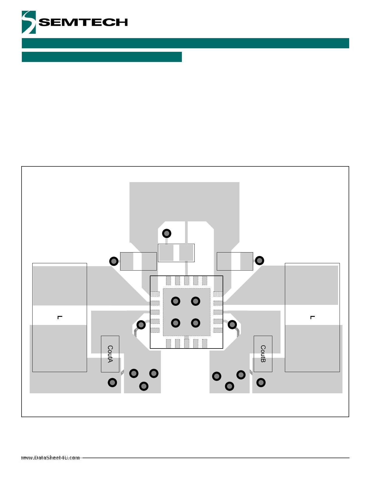
PCB Layout Considerations
Poor layout can degrade the performance of the DC-DC converter and can be a contributory factor in EMI problems,
ground bounce, thermal issues, and resistive voltage losses. Poor regulation and instability can result.
The following design rules are recommended:
1. Place the inductor and filter capacitors as close to the device as possible and use short wide traces between the
power components.
2. Route the output voltage feedback path away from inductor and LX node to minimize noise and magnetic
interference.
3. Use a ground plane to further reduce noise interference on sensitive circuit nodes.
VIN
CinA
CinR
LXA
GND
SC198
CinB
LXB
GND
VOUTA
Note:
Control pin routings are not shown.
© 2007 Semtech Corp.
11
VOUTB
www.semtech.com
11 Page | ||
| Páginas | Total 16 Páginas | |
| PDF Descargar | [ Datasheet SC198.PDF ] | |
Hoja de datos destacado
| Número de pieza | Descripción | Fabricantes |
| SC190 | Synchronous Buck Converter | Semtech |
| SC191 | Low Supply Ripple Synchronous Buck Conversion Regulator | Semtech |
| SC192 | Synchronous Buck Converter | Semtech |
| SC194A | 1A Synchronous Buck Converter | Semtech |
| Número de pieza | Descripción | Fabricantes |
| SLA6805M | High Voltage 3 phase Motor Driver IC. |
Sanken |
| SDC1742 | 12- and 14-Bit Hybrid Synchro / Resolver-to-Digital Converters. |
Analog Devices |
|
DataSheet.es es una pagina web que funciona como un repositorio de manuales o hoja de datos de muchos de los productos más populares, |
| DataSheet.es | 2020 | Privacy Policy | Contacto | Buscar |
