|
|
|
PDF NTMS4117N Data sheet ( Hoja de datos )
| Número de pieza | NTMS4117N | |
| Descripción | Power MOSFET ( Transistor ) | |
| Fabricantes | ON Semiconductor | |
| Logotipo | ||
Hay una vista previa y un enlace de descarga de NTMS4117N (archivo pdf) en la parte inferior de esta página. Total 4 Páginas | ||
|
No Preview Available !
NTMS4117N
Product Preview
Power MOSFET
30 V, 16 A, Single N−Channel, SO−8
Features
• Low RDS(on)
• Fast Switching Times
• Pb−Free Package is Available
Applications
• Notebooks, Graphics Cards
• Low Side Switch
• DC−DC
MAXIMUM RATINGS (TJ = 25°C unless otherwise noted)
Parameter
Symbol Value Unit
Drain−to−Source Voltage
Gate−to−Source Voltage
Continuous Drain
Current (Note 1)
Steady
State
Power Dissipation
(Note 1)
t v10 s
Steady
State
t v10 s
TA = 25°C
TA = 85°C
TA = 25°C
TA = 25°C
VDSS
VGS
ID
PD
30
$20
13.3
9.6
16
1.6
2.3
V
V
A
W
Continuous Drain
Current (Note 2)
Power Dissipation
(Note 2)
Steady
State
TA = 25°C
TA = 85°C
TA = 25°C
ID
PD
9.9 A
7.1
0.9 W
Pulsed Drain Current
tp = 10 ms
Operating Junction and Storage Temperature
IDM
TJ, Tstg
48
−55 to
150
A
°C
Source Current (Body Diode)
Single Pulse Drain−to−Source Avalanche
Energy
IS 2.9 A
EAS TBD mJ
Lead Temperature for Soldering Purposes
(1/8″ from case for 10 s)
TL 260 °C
THERMAL RESISTANCE MAXIMUM RATINGS
Parameter
Symbol Value Unit
Junction−to−Ambient − Steady State (Note 1)
RqJA
79 °C/W
Junction−to−Ambient − t v10 s (Note 1)
RqJA
53.5
Junction−to−Ambient − Steady State (Note 2)
RqJA
142.5
Maximum ratings are those values beyond which device damage can occur.
Maximum ratings applied to the device are individual stress limit values (not
normal operating conditions) and are not valid simultaneously. If these limits are
exceeded, device functional operation is not implied, damage may occur and
reliability may be affected.
1. Surface mounted on FR4 board using 1 in sq pad size
(Cu area 1.127 in sq [1 oz] including traces).
2. Surface mounted on FR4 board using the minimum recommended pad size
(Cu area = TBD in sq).
This document contains information on a product under development. ON Semiconductor
reserves the right to change or discontinue this product without notice.
www.DataSheet4U.com
http://onsemi.com
V(BR)DSS
30 V
RDS(on) TYP
4.0 mW @ 10 V
5.5 mW @ 4.5 V
ID MAX
(Note 1)
16 A
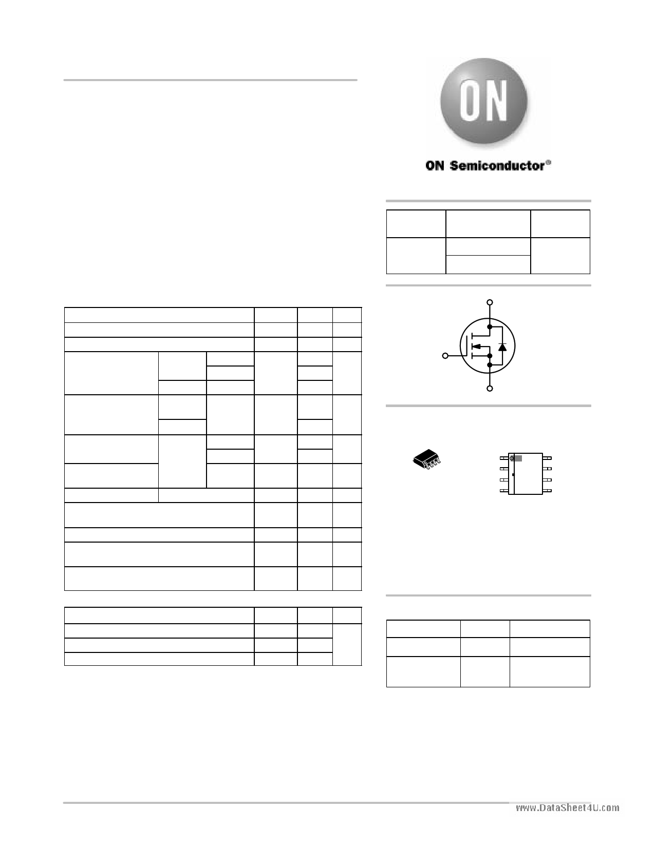
D
G
S
MARKING DIAGRAM/
PIN ASSIGNMENT
8
1
SO−8
CASE 751
STYLE 12
1
Source
Source
Source
Gate
8
Drain
Drain
Drain
Drain
(Top View)
4117N = Specific Device Code
A = Assembly Location
L = Wafer Lot
Y = Year
W = Work Week
G = Pb−Free Package
ORDERING INFORMATION
Device
Package
Shipping†
NTMS4117NR2
SO−8 2500/Tape & Reel
NTMS4117NR2G SO−8 2500/Tape & Reel
(Pb−Free)
†For information on tape and reel specifications,
including part orientation and tape sizes, please
refer to our Tape and Reel Packaging Specifications
Brochure, BRD8011/D.
© Semiconductor Components Industries, LLC, 2005
May, 2005 − Rev. P1
1
Publication Order Number:
NTMS4117N/D
1 page | ||
| Páginas | Total 4 Páginas | |
| PDF Descargar | [ Datasheet NTMS4117N.PDF ] | |
Hoja de datos destacado
| Número de pieza | Descripción | Fabricantes |
| NTMS4117N | Power MOSFET ( Transistor ) | ON Semiconductor |
| Número de pieza | Descripción | Fabricantes |
| SLA6805M | High Voltage 3 phase Motor Driver IC. |
Sanken |
| SDC1742 | 12- and 14-Bit Hybrid Synchro / Resolver-to-Digital Converters. |
Analog Devices |
|
DataSheet.es es una pagina web que funciona como un repositorio de manuales o hoja de datos de muchos de los productos más populares, |
| DataSheet.es | 2020 | Privacy Policy | Contacto | Buscar |