|
|
|
PDF NDP10N62Z Data sheet ( Hoja de datos )
| Número de pieza | NDP10N62Z | |
| Descripción | N-Channel Power MOSFET / Transistor | |
| Fabricantes | ON Semiconductor | |
| Logotipo | ||
Hay una vista previa y un enlace de descarga de NDP10N62Z (archivo pdf) en la parte inferior de esta página. Total 6 Páginas | ||
|
No Preview Available !
NDF10N62Z, NDP10N62Z
www.DataSheet4U.com
N-Channel Power MOSFET
620 V, 0.65 W
Features
• Low ON Resistance
• Low Gate Charge
• Zener Diode−protected Gate
• 100% Avalanche Tested
• These Devices are Pb−Free and RoHS Compliant
ABSOLUTE MAXIMUM RATINGS (TC = 25°C unless otherwise noted)
Rating
Symbol NDF10N62Z NDP10N62Z Unit
Drain−to−Source Voltage
Continuous Drain Current,
RqJC
Continuous Drain Current
RqJC, TA = 100°C
Pulsed Drain Current,
VGS @ 10 V
Power Dissipation, RqJC
(Note 1)
VDSS
ID
ID
IDM
PD
620 (Note 1)
10 (Note 2)
5.7 (Note 2)
36 (Note 2)
36 125
V
A
A
A
W
Gate−to−Source Voltage
Single Pulse Avalanche
Energy, ID = 10 A
ESD (HBM)
(JESD22−A114)
VGS
EAS
Vesd
±30
300
3900
V
mJ
V
RMS Isolation Voltage
(t = 0.3 sec., R.H. ≤ 30%,
TA = 25°C) (Figure 14)
Peak Diode Recovery
VISO
dv/dt
4500
4.5 (Note 3)
V
V/ns
Continuous Source
Current (Body Diode)
IS
10 A
Maximum Temperature for
Soldering Leads
TL
260 °C
Operating Junction and
TJ, Tstg
Storage Temperature Range
−55 to 150
°C
Stresses exceeding Maximum Ratings may damage the device. Maximum
Ratings are stress ratings only. Functional operation above the Recommended
Operating Conditions is not implied. Extended exposure to stresses above the
Recommended Operating Conditions may affect device reliability.
1. Surface mounted on FR4 board using 1″ sq. pad size,
(Cu area = 1.127 in sq [2 oz] including traces)
2. Limited by maximum junction temperature
3. IS ≤ 10 A, di/dt ≤ 200 A/ms, VDD = 80% BVDSS
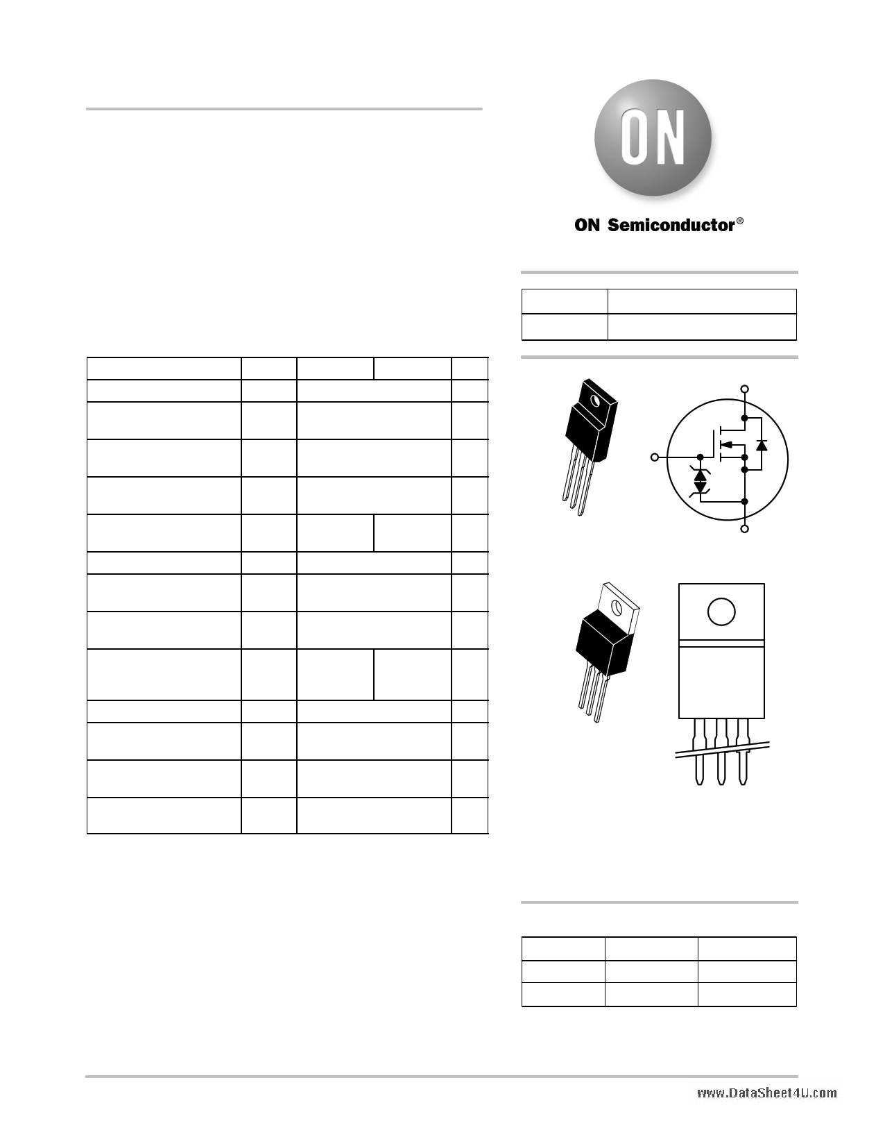
http://onsemi.com
VDSS
620 V
RDS(ON) (TYP) @ 5 A
0.65 Ω
N−Channel
D (2)
G (1)
TO−220FP
CASE 221D
STYLE 1
S (3)
MARKING
DIAGRAM
TO−220AB
CASE 221A
STYLE 5
NDF10N62ZG
or
NDP10N62ZG
AYWW
Gate
Source
Drain
A = Location Code
Y = Year
WW = Work Week
G = Pb−Free Package
ORDERING INFORMATION
Device
NDF10N62ZG
NDP10N62ZG
Package
TO−220FP
TO−220AB
Shipping
50 Units/Rail
In Development
© Semiconductor Components Industries, LLC, 2010
April, 2010 − Rev. 0
1
Publication Order Number:
NDF10N62Z/D
1 page 
NDF10N62Z, NDP10N62Z
TYPICAL CHARACTERISTICS
10
Duty Cycle = 50%
1 20%
10%
5%
0.1 2%
1%
0.01
Single Pulse Simulation
0.001
0.000001 0.00001
0.0001
0.001
0.01
0.1
1
PULSE TIME (sec)
Figure 13. Thermal Impedance for NDF10N62Z
www.DataSheet4U.com
RqJC Steady State = 3.4°C/W
10 100 1000
LEADS
HEATSINK
0.110″ MIN
Figure 14. Isolation Test Diagram
Measurement made between leads and heatsink with all leads shorted together.
*For additional mounting information, please download the ON Semiconductor
Soldering and Mounting Techniques Reference Manual, SOLDERRM/D.
http://onsemi.com
5
5 Page | ||
| Páginas | Total 6 Páginas | |
| PDF Descargar | [ Datasheet NDP10N62Z.PDF ] | |
Hoja de datos destacado
| Número de pieza | Descripción | Fabricantes |
| NDP10N62Z | N-Channel Power MOSFET / Transistor | ON Semiconductor |
| Número de pieza | Descripción | Fabricantes |
| SLA6805M | High Voltage 3 phase Motor Driver IC. |
Sanken |
| SDC1742 | 12- and 14-Bit Hybrid Synchro / Resolver-to-Digital Converters. |
Analog Devices |
|
DataSheet.es es una pagina web que funciona como un repositorio de manuales o hoja de datos de muchos de los productos más populares, |
| DataSheet.es | 2020 | Privacy Policy | Contacto | Buscar |