|
|
|
PDF CAT34TS02 Data sheet ( Hoja de datos )
| Número de pieza | CAT34TS02 | |
| Descripción | Digital Output Temperature Sensor | |
| Fabricantes | ON Semiconductor | |
| Logotipo | ||
Hay una vista previa y un enlace de descarga de CAT34TS02 (archivo pdf) en la parte inferior de esta página. Total 21 Páginas | ||
|
No Preview Available !
CAT34TS02
Digital Output Temperature
Sensor with On-board SPD
EEPROM
Description
The CAT34TS02 combines a JC42.4 compliant Temperature Sensor
(TS) with 2−Kb of Serial Presence Detect (SPD) EEPROM.
The TS measures temperature at least 10 times every second.
Temperature readings can be retrieved by the host via the serial
interface, and are compared to high, low and critical trigger limits
stored into internal registers. Over or under limit conditions can be
signaled on the open−drain EVENT pin.
The integrated 2−Kb SPD EEPROM is internally organized as 16
pages of 16 bytes each, for a total of 256 bytes. It features a page write
buffer and supports both the Standard (100 kHz) as well as Fast
(400 kHz) I2C protocol.
Write operations to the lower half memory can be inhibited via
software commands. The CAT34TS02 features Permanent, as well as
Reversible Software Write Protection, as defined for DDR3 DIMMs.
Features
• JEDEC JC42.4 Compliant Temperature Sensor
• Temperature Range: −20°C to +125°C
• DDR3 DIMM Compliant SPD EEPROM
• Supply Range: 3.3 V ± 10%
• I2C / SMBus Interface
• Schmitt Triggers and Noise Suppression Filters on SCL and SDA
Inputs
• Low Power CMOS Technology
• 2 x 3 x 0.75 mm TDFN Package and 2 x 3 x 0.5 mm UDFN Package
• These Devices are Pb−Free and are RoHS Compliant
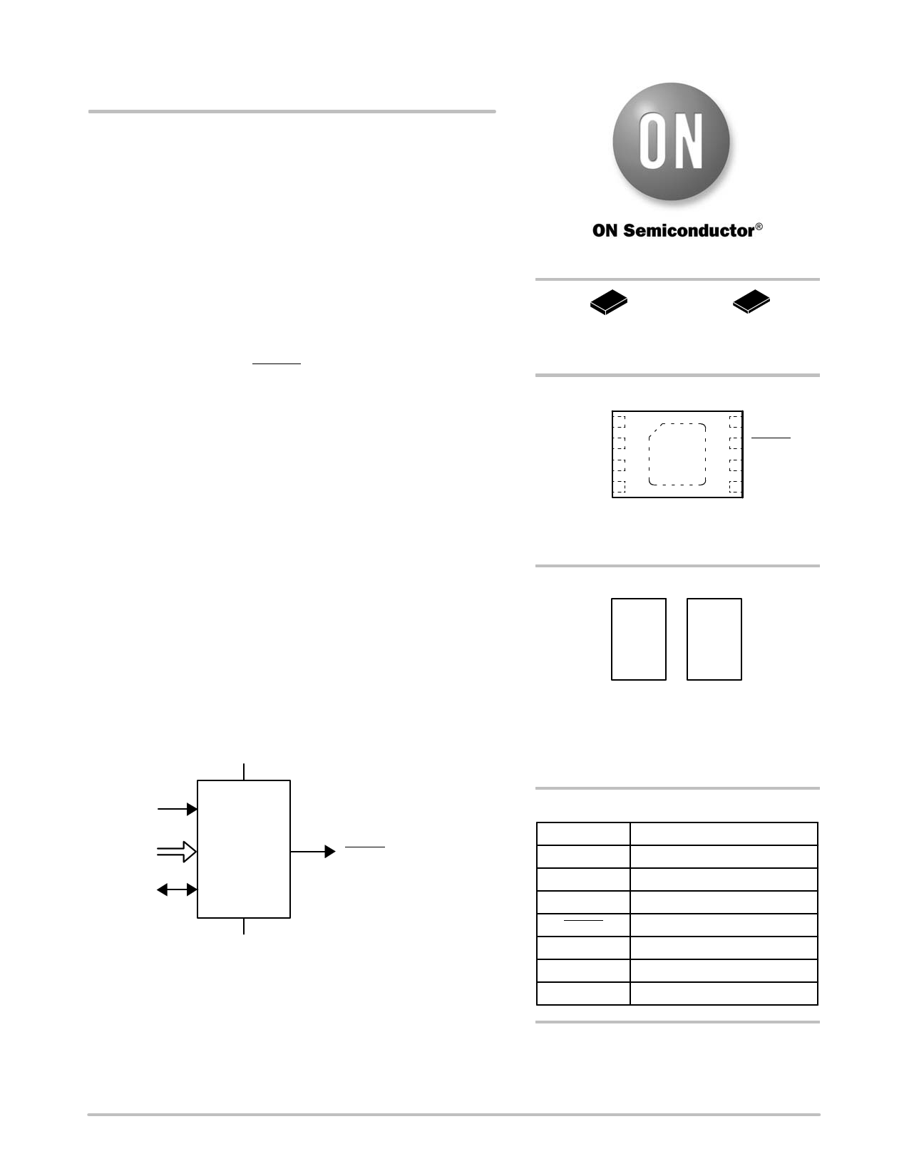
VCC
SCL
A2, A1, A0
SDA
CAT34TS02
EVENT
VSS
Figure 1. Functional Symbol
http://onsemi.com
TDFN−8
VP2 SUFFIX
CASE 511AK
UDFN−8
HU4 SUFFIX
CASE 517AZ
PIN CONFIGURATION
A0 1
A1
A2
VSS
VCC
EVENT
SCL
SDA
(Top View)
For the location of Pin 1, please consult the
corresponding package drawing.
MARKING DIAGRAM
TDFN−8
GTX
ALL
YM
G
TSU
ALL
YM
G
UDFN−8
GTX, TSU = Specific Device Code
A = Assembly Location Code
LL = Assembly Lot Number (Last Two Digits)
Y = Production Year (Last Digit)
M = Production Month (1 − 9, O, N, D)
G = Pb−Free Package
PIN FUNCTIONS
Pin Name
A0, A1, A2
SDA
SCL
Function
Device Address Input
Serial Data Input/Output
Serial Clock Input
EVENT
Open−drain Event Output
VCC
VSS
DAP
Power Supply
Ground
Backside Exposed DAP at VSS
ORDERING INFORMATION
See detailed ordering and shipping information in the package
dimensions section on page 21 of this data sheet.
© Semiconductor Components Industries, LLC, 2014
June, 2014 − Rev. 12
1
Publication Order Number:
CAT34TS02/D
1 page 
CAT34TS02
TYPICAL PERFORMANCE CHARACTERISTICS
(VCC = 3.3 V, TA = −20°C to +125°C, unless otherwise specified.)
44
33
2
Part # 2
1
2
Part # 2
1
00
−1
Part # 1
−2
−1
Part # 1
−2
−3
−4
−25
0
25 50
75 100 125
TAMB (°C)
Figure 8. Temperature Read−Out Error (Rev. B)
−3
−4
−25
0
25 50 75 100 125
TAMB (°C)
Figure 9. Temperature Read−Out Error (Rev. C)
80
70
60
50
40
30
20
−25
0
25 50 75 100
TAMB (°C)
Figure 10. A/D Conversion Time (Rev. B)
125
80
70
60
50
40
30
20
−25
0
25 50 75 100 125
TAMB (°C)
Figure 11. A/D Conversion Time (Rev. C)
5.0
4.5
4.0
3.5
3.0
2.5
2.0
−25
0 25 50 75 100
TAMB (°C)
Figure 12. EEPROM Write Time (Rev. B)
125
3.5
3.0
2.5
2.0
1.5
1.0
0.5
−25
0 25 50 75 100
TAMB (°C)
Figure 13. EEPROM Write Time (Rev. C)
125
http://onsemi.com
5
5 Page 
CAT34TS02
BUS ACTIVITY:
MASTER
S
T
A
R
T
SDA LINE S
SLAVE
SPD
SLAVE
ADDRESS
BYTE
ADDRESS (n)
S
T
A SLAVE
R ADDRESS
T
S
AA
CC
KK
A
C
K
Figure 29a. EEPROM Selective Read
DATA n
N
OS
AT
CO
KP
P
BUS ACTIVITY:
MASTER
S
T
A
R
T
SDA LINE S
SLAVE
TS
SLAVE
ADDRESS
REGISTER
ADDRESS
S
T
A SLAVE
R ADDRESS
T
S
A
C
K
AA
CC
KK
A
C DATA (MSB)
K
Figure 29b. Temperature Sensor Selective Read
N
OS
AT
CO
KP
P
DATA (LSB)
BUS ACTIVITY:
SPD
SLAVE
MASTER ADDRESS
SDA LINE
SLAVE
A
C
K
AAA
CCC
KKK
DATA n
DATA n+1
DATA n+2
Figure 30. EEPROM Sequential Read
N
OS
AT
CO
KP
P
DATA n+x
Software Write Protection
The lower half of memory (first 128 bytes) can be
protected against Write requests by setting one of two
Software Write Protection (SWP) flags.
The Permanent Software Write Protection (PSWP) flag
can be set or read while all address pins are at regular CMOS
levels (GND or VCC), whereas the very high voltage VHV
must be present on address pin A0 to set, clear or read the
Reversible Software Write Protection (RSWP) flag. The
D.C. OPERATING CONDITIONS for RSWP operations
are shown in Table 7.
The SWP commands are listed in Table 8. All commands
are preceded by a START and terminated with a STOP,
following the ACK or NoACK from the CAT34TS02. All
SWP related Slave addresses use the pre−amble: 0110 (6h),
instead of the regular 1010 (Ah) used for memory access.
For PSWP commands, the three address pins can be at any
logic level, whereas for RSWP commands the address pins
must be at pre−assigned logic levels.
VHV is interpreted as logic ‘1’. The VHV condition must
be established on pin A0 before the START and
maintained just beyond the STOP. Otherwise an RSWP
request could be interpreted by the CAT34TS02 as a
PSWP request.
The SWP Slave addresses follow the standard I2C
convention, i.e. to read the state of the SWP flag, the LSB of
the Slave address must be ‘1’, and to set or clear a flag, it
must be ‘0’. For Write commands a dummy byte address and
dummy data byte must be provided (Figure 31). In contrast
to a regular memory Read, a SWP Read does not return data.
Instead the CAT34TS02 will respond with NoACK if the
flag is set and with ACK if the flag is not set. Therefore, the
Master can immediately follow up with a STOP, as there is
no meaningful data following the ACK interval (Figure 32).
http://onsemi.com
11
11 Page | ||
| Páginas | Total 21 Páginas | |
| PDF Descargar | [ Datasheet CAT34TS02.PDF ] | |
Hoja de datos destacado
| Número de pieza | Descripción | Fabricantes |
| CAT34TS00 | 1.8V Digital Temperature Sensor | ON Semiconductor |
| CAT34TS02 | Digital Output Temperature Sensor | ON Semiconductor |
| CAT34TS04 | Digital Output Temperature Sensor | ON Semiconductor |
| Número de pieza | Descripción | Fabricantes |
| SLA6805M | High Voltage 3 phase Motor Driver IC. |
Sanken |
| SDC1742 | 12- and 14-Bit Hybrid Synchro / Resolver-to-Digital Converters. |
Analog Devices |
|
DataSheet.es es una pagina web que funciona como un repositorio de manuales o hoja de datos de muchos de los productos más populares, |
| DataSheet.es | 2020 | Privacy Policy | Contacto | Buscar |