|
|
|
PDF N04L63W2A Data sheet ( Hoja de datos )
| Número de pieza | N04L63W2A | |
| Descripción | 4Mb Ultra-Low Power Asynchronous CMOS SRAM 256K x 16 bit | |
| Fabricantes | ON Semiconductor | |
| Logotipo | ||
Hay una vista previa y un enlace de descarga de N04L63W2A (archivo pdf) en la parte inferior de esta página. Total 10 Páginas | ||
|
No Preview Available !
N04L63W2Awww.DataSheet4U.com
4Mb Ultra-Low Power Asynchronous CMOS SRAM
256K × 16 bit
Overview
Features
The N04L63W2A is an integrated memory device
containing a 4 Mbit Static Random Access Memory
organized as 262,144 words by 16 bits. The device
is designed and fabricated using ON
Semiconductor’s advanced CMOS technology to
provide both high-speed performance and ultra-low
power. The device operates with two chip enable
(CE1 and CE2) controls and output enable (OE) to
allow for easy memory expansion. Byte controls
(UB and LB) allow the upper and lower bytes to be
accessed independently and can also be used to
deselect the device. The N04L63W2A is optimal
for various applications where low-power is critical
such as battery backup and hand-held devices.
The device can operate over a very wide
temperature range of -40oC to +85oC and is
available in JEDEC standard packages compatible
with other standard 256Kb x 16 SRAMs
Product Family
• Single Wide Power Supply Range
2.3 to 3.6 Volts
• Very low standby current
4.0µA at 3.0V (Typical)
• Very low operating current
2.0mA at 3.0V and 1µs (Typical)
• Very low Page Mode operating current
0.8mA at 3.0V and 1µs (Typical)
• Simple memory control
Dual Chip Enables (CE1 and CE2)
Output Enable (OE) for memory expansion
• Low voltage data retention
Vcc = 1.8V
• Very fast output enable access time
25ns OE access time
• Automatic power down to standby mode
• TTL compatible three-state output driver
• Compact space saving BGA package avail-
able
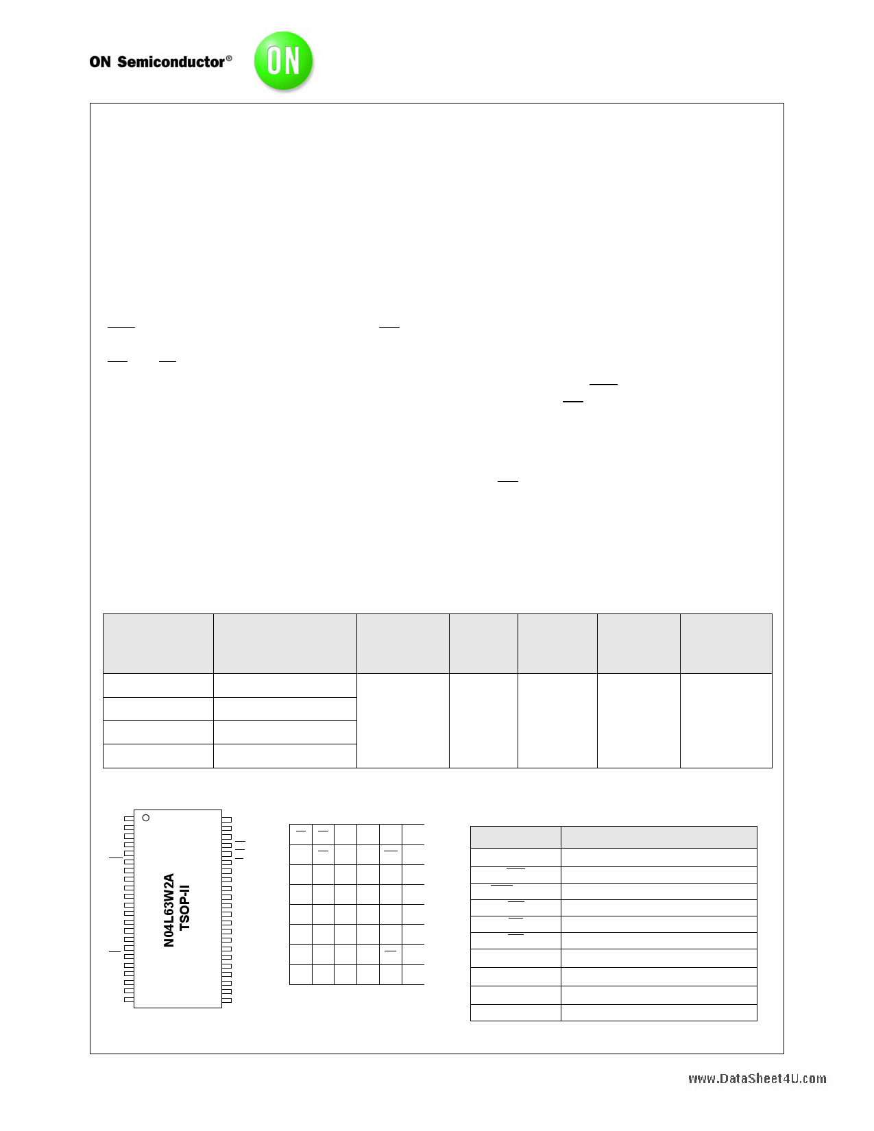
Part Number
N04L63W2AB
N04L63W2AT
N04L63W2AB2
N04L63W2AT2
Package Type
48 - BGA
44 - TSOP II
48 - BGA Green
44 - TSOP II Green
Operating
Temperature
Power
Supply
(Vcc)
Speed
Options
Standby
Operating
Current (ISB), Current (Icc),
Typical
Typical
-40oC to +85oC 2.3V - 3.6V
70ns @ 2.7V
55ns @ 2.7V
4 µA
2 mA @ 1MHz
Pin Configuration
A4
A3
A2
A1
A0
CE1
I/O0
I/O1
I/O2
I/O3
VCC
VSS
I/O4
I/O5
I/O6
I/O7
WE
A16
A15
A14
A13
A12
1
2
3
4
5
6
7
8
9
10
11
12
13
14
15
16
17
18
19
20
21
22
PIN
ONE
44 A5
43 A6
42 A7
41 OE
40 UB
39 LB
38 I/O15
37 I/O14
36 I/O13
35 I/O12
34 VSS
33 VCC
32 I/O11
31 I/O10
30 I/O9
29 I/O8
28 CE2
27 A8
26 A9
25 A10
24 A11
23 A17
123456
A LB OE A0 A1 A2 CE2
B I/O8 UB A3 A4 CE1 I/O0
C I/O9 I/O10 A5 A6 I/O1 I/O2
D VSS I/O11 A17 A7 I/O3 VCC
E VCC I/O12 NC A16 I/O4 VSS
F I/O14 I/O13 A14 A15 I/O5 I/O6
G I/O15 NC A12 A13 WE I/O7
H NC A8 A9 A10 A11 NC
48 Pin BGA (top)
6 x 8 mm
Pin Descriptions
Pin Name
A0-A17
WE
CE1, CE2
OE
LB
UB
I/O0-I/O15
VCC
VSS
NC
Pin Function
Address Inputs
Write Enable Input
Chip Enable Input
Output Enable Input
Lower Byte Enable Input
Upper Byte Enable Input
Data Inputs/Outputs
Power
Ground
Not Connected
©2008 SCILLC. All rights reserved.
July 2008 - Rev. 10
Publication Order Number:
N04L63W2A/D
1 page 
N04L63W2A
Timing Test Conditions
Item
Input Pulse Level
Input Rise and Fall Time
Input and Output Timing Reference Levels
Output Load
Operating Temperature
www.DataShe
0.1VCC to 0.9 VCC
5ns
0.5 VCC
CL = 30pF
-40 to +85 oC
Timing
Item
Symbol
Read Cycle Time
tRC
Address Access Time
tAA
Chip Enable to Valid Output
tCO
Output Enable to Valid Output
tOE
Byte Select to Valid Output
tLB, tUB
Chip Enable to Low-Z output
tLZ
Output Enable to Low-Z Output
tOLZ
Byte Select to Low-Z Output
tBZ
Chip Disable to High-Z Output
tHZ
Output Disable to High-Z Output tOHZ
Byte Select Disable to High-Z Output tBHZ
Output Hold from Address Change tOH
-70
2.3 - 2.65 V
2.7 - 3.6 V
Min. Max. Min. Max.
85 70
85 70
85 70
30 25
85 70
10 10
55
10 10
0 20 0 20
0 20 0 20
0 20 0 20
10 10
-55
2.7 - 3.6 V
Min. Max.
55
55
55
25
55
10
5
10
0 20
0 20
0 20
10
Units
ns
ns
ns
ns
ns
ns
ns
ns
ns
ns
ns
ns
Write Cycle Time
tWC 85
70
55 ns
Chip Enable to End of Write
tCW 50
50
45 ns
Address Valid to End of Write tAW 50 50 45 ns
Byte Select to End of Write
tBW 50
50
45 ns
Write Pulse Width
tWP 40
40
40 ns
Address Setup Time
tAS 0
0
0 ns
Write Recovery Time
tWR 0
0
0 ns
Write to High-Z Output
tWHZ
20
20
20 ns
Data to Write Time Overlap
tDW 40
40
40 ns
Data Hold from Write Time
tDH 0
0
0 ns
End Write to Low-Z Output
tOW 5
5
5 ns
Rev. 10 | Page 5 of 10 | www.onsemi.com
5 Page | ||
| Páginas | Total 10 Páginas | |
| PDF Descargar | [ Datasheet N04L63W2A.PDF ] | |
Hoja de datos destacado
| Número de pieza | Descripción | Fabricantes |
| N04L63W2A | 4Mb Ultra-Low Power Asynchronous CMOS SRAM 256K x 16 bit | ON Semiconductor |
| Número de pieza | Descripción | Fabricantes |
| SLA6805M | High Voltage 3 phase Motor Driver IC. |
Sanken |
| SDC1742 | 12- and 14-Bit Hybrid Synchro / Resolver-to-Digital Converters. |
Analog Devices |
|
DataSheet.es es una pagina web que funciona como un repositorio de manuales o hoja de datos de muchos de los productos más populares, |
| DataSheet.es | 2020 | Privacy Policy | Contacto | Buscar |