|
|
PDF NB7V52M Data sheet ( Hoja de datos )
| Número de pieza | NB7V52M | |
| Descripción | 1.8V / 2.5V Differential D Flip-Flop w/ Reset and CML Outputs | |
| Fabricantes | ON Semiconductor | |
| Logotipo | ||
Hay una vista previa y un enlace de descarga de NB7V52M (archivo pdf) en la parte inferior de esta página. Total 10 Páginas | ||
|
No Preview Available !
NB7V52M
1.8V / 2.5V Differential D
Flip-Flop w/ Reset and CML
Outputs
Multi−Level Inputs w/ Internal Termination
Description
The NB7V52M is a 10 GHz differential D flip−flop with a
differential asynchronous Reset. The differential D/D, CLK/CLK and
R/R inputs incorporate dual internal 50 W termination resistors and
will accept LVPECL, CML, LVDS logic levels.
When Clock transitions from logic Low to High, Data will be
transferred to the differential CML outputs. The differential Clock
inputs allow the NB7V52M to also be used as a negative edge
triggered device.
The 16 mA differential CML outputs provide matching internal
50 W termination and produce 400 mV output swings when externally
receiver terminated with a 50 W resistor to VCC.
The NB7V52M is offered in a low profile 3 mm x 3 mm 16−pin
QFN package. The NB7V52M is a member of the GigaComm™
family of high performance clock products. Application notes,
models, and support documentation are available at
www.onsemi.com.
Features
• Maximum Input Clock Frequency > 10 GHz
• Maximum Input Data Rate > 10 Gb/s
• Random Clock Jitter < 0.8 ps RMS, Max
• 200 ps Typical Propagation Delay
• 35 ps Typical Rise and Fall Times
• Differential CML Outputs, 400 mV Peak−to−Peak, Typical
• Operating Range: VCC = 1.71 V to 2.625 V with VEE = 0 V
• Internal 50 W Input Termination Resistors
• QFN−16 Package, 3mm x 3mm
• −40°C to +85°C Ambient Operating Temperature
• These are Pb−Free Devices
http://onsemi.com
1
QFN−16
MN SUFFIX
CASE 485G
MARKING
DIAGRAM*
16
1
NB7V
52M
ALYWG
G
A = Assembly Location
L = Wafer Lot
Y = Year
W = Work Week
G = Pb−Free Package
(Note: Microdot may be in either location)
*For additional marking information, refer to
Application Note AND8002/D.
VTD
D
D
VTD
VTCLK
D Flip−Flop
CLK
CLK
VTCLK
RESET
VTR R R VTR
Figure 1. Logic Diagram
Q
Q
ORDERING INFORMATION
See detailed ordering and shipping information in the package
dimensions section on page 9 of this data sheet.
© Semiconductor Components Industries, LLC, 2014
July, 2014 − Rev. 4
1
Publication Order Number:
NB7V52M/D
1 page 
NB7V52M
Table 5. AC CHARACTERISTICS VCC = 1.71 V to 2.625 V; VEE = 0 V; TA = −40°C to 85°C (Note 10)
Symbol
Characteristic
Min Typ
Max
Unit
fMAX
fDATA MAX
VOUTPP
Maximum Input Clock Frequency
Maximum Input Data Rate (PRBS23)
Output Voltage Amplitude (@ VINPPmin)
(See Figures 3 and 10, Note 11)
fin ≤ 7 GHz
fin ≤ 10 GHz
10 12
10 12
300 400
250 400
GHz
Gbps
mV
tPLH,
tPHL
Propagation Delay to Differential Outputs, @ 1 GHz,
Measured at Differential Cross−point
CLK/CLK to Q/Q
R/R to Q/Q
200 350
300 600
ps
tS
tH
tRR
tPW
tJITTER
VINPP
tr,, tf
Setup Time (D to CLK)
Hold Time (D to CLK)
Reset Recovery
Minimum Pulse Width
R/R
RJ – Output Random Jitter (Note 12)
fin v 10 GHz
Input Voltage Swing (Differential Configuration) (Note 13)
Output Rise/Fall Times @ 1 GHz (20% − 80%),
Q, Q
40 15
ps
50 20
ps
275 200
ps
1 ns
0.2 0.8 ps RMS
100
1200
mV
20 35 50
ps
NOTE: Device will meet the specifications after thermal equilibrium has been established when mounted in a test socket or printed circuit
board with maintained transverse airflow greater than 500 lfpm. Electrical parameters are guaranteed only over the declared
operating temperature range. Functional operation of the device exceeding these conditions is not implied. Device specification limit
values are applied individually under normal operating conditions and not valid simultaneously.
10. Measured using a 400 mV VINPP source, 50% duty cycle clock source. All output loading with external 50 W to VCC. Input edge rates
w40 ps (20% − 80%).
11. Output voltage swing is a single−ended measurement operating in differential mode.
12. Additive RMS jitter with 50% duty cycle clock signal.
13. Input voltage swing is a single−ended measurement operating in differential mode.
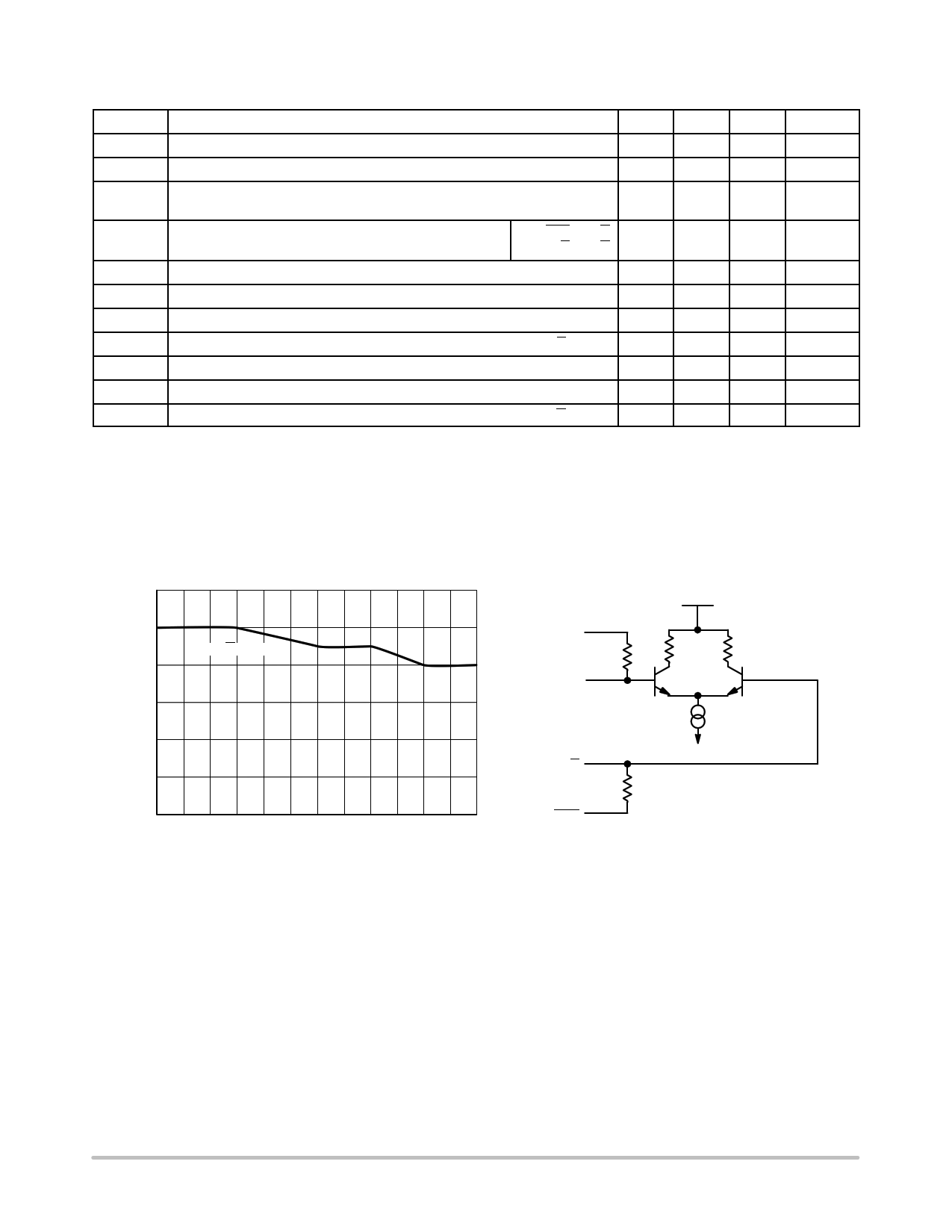
500 VCC
450
Q/Q Output
400
350
300
250
200
0 1 2 3 4 5 6 7 8 9 10 11 12
fin, Clock Input Frequency (GHz)
Figure 3. Clock Output Voltage Amplitude
(VOUTPP) vs. Input Frequency (fin) at Ambient
Temperature (Typ)
VTD
50 W
D
RTIN
RC
RC
I
D
50 W RTIN
VTD
Figure 4. Simplified Input Structure
http://onsemi.com
5
5 Page | ||
| Páginas | Total 10 Páginas | |
| PDF Descargar | [ Datasheet NB7V52M.PDF ] | |
Hoja de datos destacado
| Número de pieza | Descripción | Fabricantes |
| NB7V52M | 1.8V / 2.5V Differential D Flip-Flop w/ Reset and CML Outputs | ON Semiconductor |
| Número de pieza | Descripción | Fabricantes |
| SLA6805M | High Voltage 3 phase Motor Driver IC. |
Sanken |
| SDC1742 | 12- and 14-Bit Hybrid Synchro / Resolver-to-Digital Converters. |
Analog Devices |
|
DataSheet.es es una pagina web que funciona como un repositorio de manuales o hoja de datos de muchos de los productos más populares, |
| DataSheet.es | 2020 | Privacy Policy | Contacto | Buscar |
