|
|
|
PDF NLX2G08 Data sheet ( Hoja de datos )
| Número de pieza | NLX2G08 | |
| Descripción | Dual 2-Input AND Gate | |
| Fabricantes | ON Semiconductor | |
| Logotipo | ||
Hay una vista previa y un enlace de descarga de NLX2G08 (archivo pdf) en la parte inferior de esta página. Total 5 Páginas | ||
|
No Preview Available !
NLX2G08
Dual 2-Input AND Gate
The NLX2G08 is a high performance dual 2−input AND Gate
operating from a 1.65 V to 5.5 V supply.
Features
• Extremely High Speed: tPD 2.5 ns (typical) at VCC = 5 V
• Designed for 1.65 V to 5.5 V VCC Operation
• Over Voltage Tolerant Inputs
• LVTTL Compatible − Interface Capability With 5 V TTL Logic with
VCC = 3 V
• LVCMOS Compatible
• 24 mA Balanced Output Sink and Source Capability
• Near Zero Static Supply Current Substantially Reduces System
Power Requirements
• Replacement for NC7WZ08
• Chip Complexity: FET = 124
• This is a Pb−Free Device
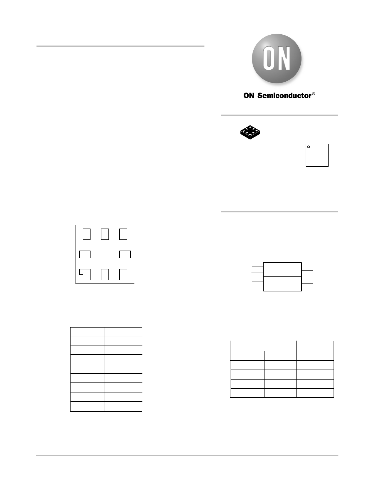
A1 B1 Y2
765
http://onsemi.com
18
UQFN8
MU SUFFIX
CASE 523AN
MARKING
DIAGRAM
1
AD MG
G
AD = Device Code
M = Date Code*
G = Pb−Free Package
(Note: Microdot may be in either location)
ORDERING INFORMATION
See detailed ordering and shipping information in the package
dimensions section on page 4 of this data sheet.
VCC 8
4 GND
1 23
Y1 B2 A2
Figure 1. Pinout
PIN ASSIGNMENT
Pin Function
1 Y1
2 B2
3 A2
4 GND
5 Y2
6 B1
7 A1
8 VCC
IEEE/IEC
A1
B1
& Y1
A2
B2
Y2
Figure 2. Logic Symbol
FUNCTION TABLE
Y = AB
Inputs
AB
LL
LH
HL
HH
H = HIGH Logic Level
L = LOW Logic Level
Output
Y
L
L
L
H
© Semiconductor Components Industries, LLC, 2009
April, 2009 − Rev. 0
www.DataSheet.in
1
Publication Order Number:
NLX2G08/D
1 page 
NLX2G08
PACKAGE DIMENSIONS
UQFN8
MU SUFFIX
CASE 523AN−01
ISSUE O
D
PIN ONE
ÉÉÉREFERENCE
ÉÉÉ2X
0.10 C
2X
0.10 C
TOP VIEW
A
B
E
0.05 C
DETAIL B (A3)
0.05 C
SIDE VIEW
A1
8X L
8X
L3
e
EXPOSED Cu
MOLD CMPD
ÇÇÇ A3
ÇÉÉÇÉÉÇÉÉA1 DETAIL B
NOTES:
1. DIMENSIONING AND TOLERANCING PER
ASME Y14.5M, 1994.
2. CONTROLLING DIMENSION: MILLIMETERS.
3. DIMENSION b APPLIES TO PLATED TERMINAL
AND IS MEASURED BETWEEN 0.15 AND
0.30 mm FROM THE TERMINAL TIP.
MILLIMETERS
DIM MIN MAX
OPTIONAL
CONSTRUCTION
A 0.45 0.60
A1 0.00 0.05
A3 0.13 REF
b 0.15 0.25
L1 L3
D 1.60 BSC
A
E 1.60 BSC
e 0.50 BSC
L 0.35 0.45
L1 −−− 0.15
C
SEATING
PLANE
b
(0.10)
DETAIL A
L3 0.25 0.35
(0.15)
SOLDERING FOOTPRINT*
OPTIONAL
CONSTRUCTION
1.70 0.50
PITCH
1
35
DETAIL A
1
7
8 8X b
0.35 1.70
BOTTOM VIEW
0.10 C A B
0.05 C NOTE 3
7X 0.25
8X
0.53
DIMENSIONS: MILLIMETERS
*For additional information on our Pb−Free strategy and soldering
details, please download the ON Semiconductor Soldering and
Mounting Techniques Reference Manual, SOLDERRM/D.
ON Semiconductor and
are registered trademarks of Semiconductor Components Industries, LLC (SCILLC). SCILLC reserves the right to make changes without further notice
to any products herein. SCILLC makes no warranty, representation or guarantee regarding the suitability of its products for any particular purpose, nor does SCILLC assume any liability
arising out of the application or use of any product or circuit, and specifically disclaims any and all liability, including without limitation special, consequential or incidental damages.
“Typical” parameters which may be provided in SCILLC data sheets and/or specifications can and do vary in different applications and actual performance may vary over time. All
operating parameters, including “Typicals” must be validated for each customer application by customer’s technical experts. SCILLC does not convey any license under its patent rights
nor the rights of others. SCILLC products are not designed, intended, or authorized for use as components in systems intended for surgical implant into the body, or other applications
intended to support or sustain life, or for any other application in which the failure of the SCILLC product could create a situation where personal injury or death may occur. Should Buyer
purchase or use SCILLC products for any such unintended or unauthorized application, Buyer shall indemnify and hold SCILLC and its officers, employees, subsidiaries, affiliates,
and distributors harmless against all claims, costs, damages, and expenses, and reasonable attorney fees arising out of, directly or indirectly, any claim of personal injury or death
associated with such unintended or unauthorized use, even if such claim alleges that SCILLC was negligent regarding the design or manufacture of the part. SCILLC is an Equal
Opportunity/Affirmative Action Employer. This literature is subject to all applicable copyright laws and is not for resale in any manner.
PUBLICATION ORDERING INFORMATION
LITERATURE FULFILLMENT:
Literature Distribution Center for ON Semiconductor
P.O. Box 5163, Denver, Colorado 80217 USA
Phone: 303−675−2175 or 800−344−3860 Toll Free USA/Canada
Fax: 303−675−2176 or 800−344−3867 Toll Free USA/Canada
Email: [email protected]
N. American Technical Support: 800−282−9855 Toll Free
USA/Canada
Europe, Middle East and Africa Technical Support:
Phone: 421 33 790 2910
Japan Customer Focus Center
Phone: 81−3−5773−3850
http://onsemi.com
5
ON Semiconductor Website: www.onsemi.com
Order Literature: http://www.onsemi.com/orderlit
For additional information, please contact your local
Sales Representative
NLX2G08/D
www.DataSheet.in
5 Page | ||
| Páginas | Total 5 Páginas | |
| PDF Descargar | [ Datasheet NLX2G08.PDF ] | |
Hoja de datos destacado
| Número de pieza | Descripción | Fabricantes |
| NLX2G00 | Dual 2-Input NAND Gate | ON Semiconductor |
| NLX2G02 | Dual 2-Input NOR Gate | ON Semiconductor |
| NLX2G04 | Dual Inverter | ON Semiconductor |
| NLX2G06 | Dual Inverter | ON Semiconductor |
| Número de pieza | Descripción | Fabricantes |
| SLA6805M | High Voltage 3 phase Motor Driver IC. |
Sanken |
| SDC1742 | 12- and 14-Bit Hybrid Synchro / Resolver-to-Digital Converters. |
Analog Devices |
|
DataSheet.es es una pagina web que funciona como un repositorio de manuales o hoja de datos de muchos de los productos más populares, |
| DataSheet.es | 2020 | Privacy Policy | Contacto | Buscar |