|
|
|
PDF CBTL03SB212 Data sheet ( Hoja de datos )
| Número de pieza | CBTL03SB212 | |
| Descripción | DisplayPort Gen2 sideband signal multiplexer | |
| Fabricantes | NXP Semiconductors | |
| Logotipo | ||
Hay una vista previa y un enlace de descarga de CBTL03SB212 (archivo pdf) en la parte inferior de esta página. Total 16 Páginas | ||
|
No Preview Available !
CBTL03SB212
DisplayPort Gen2 sideband signal multiplexer
Rev. 1 — 21 February 2011
Product data sheet
1. General description
The CBTL03SB212 is a sideband signal multiplexer for DisplayPort Gen2 applications. It
provides one differential channel capable of switching or multiplexing (bidirectional and
AC-coupled) DisplayPort 1.2 Fast AUX or AUX signal, using high-bandwidth pass-gate
technology. Additionally, it provides for switching/multiplexing of the Hot Plug Detect signal
as well as the Display Data Channel (DDC) signals, for a total of three channels.
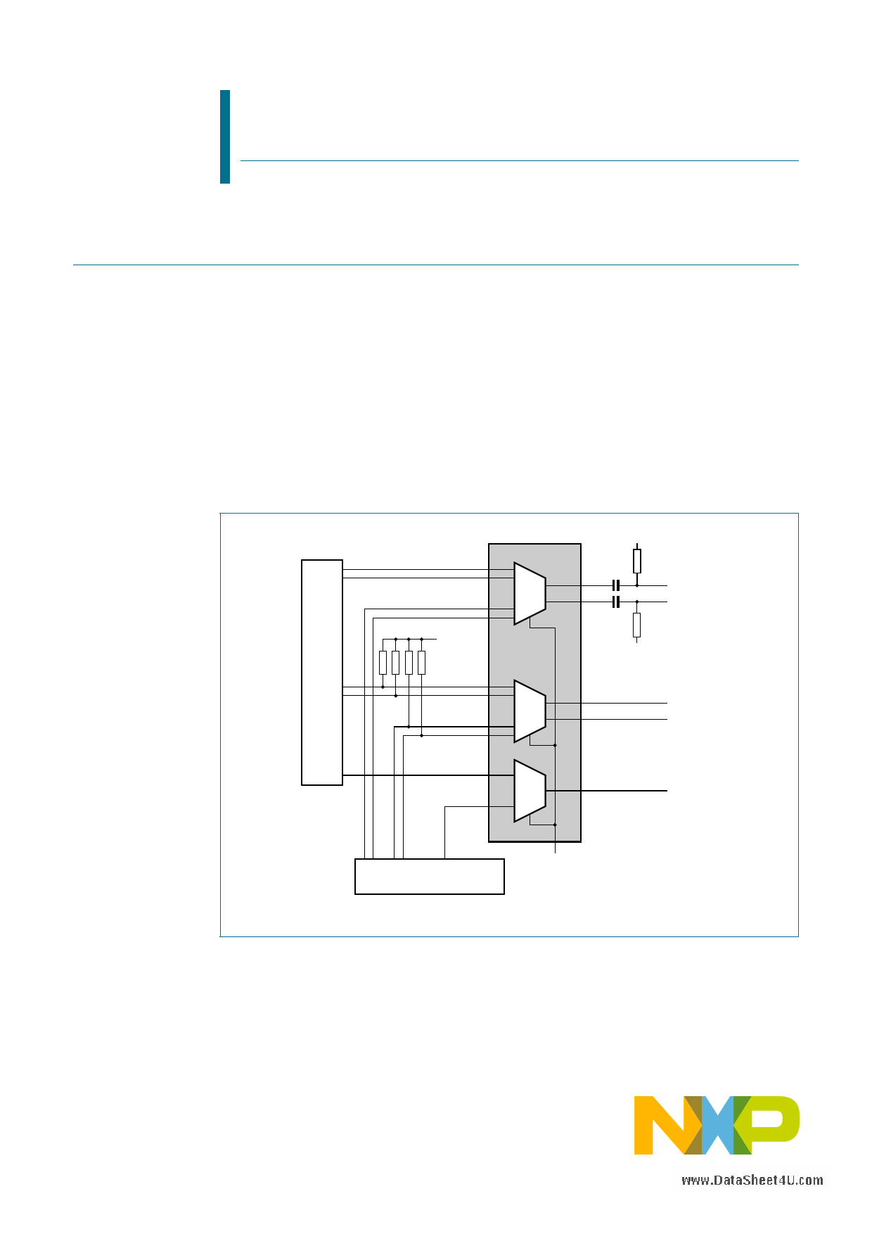
A typical application of CBTL03SB212 is on motherboards where one of two GPU display
sources needs to be selected to connect to a display sink device or connector. A controller
chip selects which path to use by setting a select signal HIGH or LOW. Due to the
non-directional nature of the signal paths (which use high-bandwidth pass-gate
technology), the CBTL03SB212 can also be used in the reverse topology, e.g., to connect
one display source device to one of two display sink devices or connectors.
GPU1
CBTL03SB212
AUX1+
AUX1−
AUX2+
2:1
MUX
AUX2−
+3.3 V
2 kΩ
DDC_CLK1
DDC_DAT1
DDC_CLK2
2:1
MUX
DDC_DAT2
HPD_1
HPD_2
2:1
MUX
GND
100 kΩ
AUX+
AUX−
100 kΩ
+3.3 V
DDC_CLK
DDC_DAT
HPD
GPU2
SEL, XSD_N
Fig 1. CBTL03SB212 application example
002aag007
www.DataSheet4U.com
1 page 
NXP Semiconductors
CBTL03SB212
DisplayPort Gen2 sideband signal multiplexer
7. Functional description
Refer to Figure 2 “Functional diagram”.
The CBTL03SB212 uses 3.3 V power supply. All signal paths are implemented using
high-bandwidth pass-gate technology, are bidirectional and no clock or reset signal is
needed for the multiplexer to function.
The switch position is selected using the select signal (SEL). The detailed operation is
described in Section 7.1.
7.1 MUX select (SEL) function
The internal multiplexer switch position is controlled by the logic inputs SEL as described
below.
Table 3.
SEL
0
1
MUX select control
Path 2
high-impedance
active
Path 1
active
high-impedance
7.2 Shutdown function
The CBTL03SB212 provides a shutdown function to minimize power consumption when
the application is not active but power to the CBTL03SB212 is provided. Pin XSD_N
(active LOW) puts all channels in Off mode (non-conducting high-impedance state) while
reducing current consumption to near-zero.
Table 4.
XSD_N
0
1
Shutdown function
State
shutdown
active
www.DataSheet4U.com
CBTL03SB212
Product data sheet
All information provided in this document is subject to legal disclaimers.
Rev. 1 — 21 February 2011
© NXP B.V. 2011. All rights reserved.
5 of 16
5 Page 
NXP Semiconductors
CBTL03SB212
DisplayPort Gen2 sideband signal multiplexer
13.4 Reflow soldering
Key characteristics in reflow soldering are:
• Lead-free versus SnPb soldering; note that a lead-free reflow process usually leads to
higher minimum peak temperatures (see Figure 5) than a SnPb process, thus
reducing the process window
• Solder paste printing issues including smearing, release, and adjusting the process
window for a mix of large and small components on one board
• Reflow temperature profile; this profile includes preheat, reflow (in which the board is
heated to the peak temperature) and cooling down. It is imperative that the peak
temperature is high enough for the solder to make reliable solder joints (a solder paste
characteristic). In addition, the peak temperature must be low enough that the
packages and/or boards are not damaged. The peak temperature of the package
depends on package thickness and volume and is classified in accordance with
Table 12 and 13
Table 12. SnPb eutectic process (from J-STD-020C)
Package thickness (mm) Package reflow temperature (°C)
Volume (mm3)
< 350
≥ 350
< 2.5
235
220
≥ 2.5
220
220
Table 13. Lead-free process (from J-STD-020C)
Package thickness (mm) Package reflow temperature (°C)
Volume (mm3)
< 350
350 to 2000
< 1.6
260 260
1.6 to 2.5
260 250
> 2.5
250 245
> 2000
260
245
245
Moisture sensitivity precautions, as indicated on the packing, must be respected at all
times.
Studies have shown that small packages reach higher temperatures during reflow
soldering, see Figure 5.
www.DataSheet4U.com
CBTL03SB212
Product data sheet
All information provided in this document is subject to legal disclaimers.
Rev. 1 — 21 February 2011
© NXP B.V. 2011. All rights reserved.
11 of 16
11 Page | ||
| Páginas | Total 16 Páginas | |
| PDF Descargar | [ Datasheet CBTL03SB212.PDF ] | |
Hoja de datos destacado
| Número de pieza | Descripción | Fabricantes |
| CBTL03SB212 | DisplayPort Gen2 sideband signal multiplexer | NXP Semiconductors |
| Número de pieza | Descripción | Fabricantes |
| SLA6805M | High Voltage 3 phase Motor Driver IC. |
Sanken |
| SDC1742 | 12- and 14-Bit Hybrid Synchro / Resolver-to-Digital Converters. |
Analog Devices |
|
DataSheet.es es una pagina web que funciona como un repositorio de manuales o hoja de datos de muchos de los productos más populares, |
| DataSheet.es | 2020 | Privacy Policy | Contacto | Buscar |