|
|
|
PDF NCP4672 Data sheet ( Hoja de datos )
| Número de pieza | NCP4672 | |
| Descripción | Dual Linear Voltage Regulators | |
| Fabricantes | ON Semiconductor | |
| Logotipo | ||
Hay una vista previa y un enlace de descarga de NCP4672 (archivo pdf) en la parte inferior de esta página. Total 8 Páginas | ||
|
No Preview Available !
NCP4672
Dual Linear Voltage
Regulators with Vin and Vout
Voltage Detector
The NCP4672 is a dual linear voltage regulator with input voltage
and output voltage detectors. This part is useful in systems where
multiple voltages are required such as for core and I/O. The NCP4672
is very accurate at 2% over full input voltage and full load current. The
NCP4672 eliminates the need for external voltage supervision due to
the two built in voltage detectors. The voltage detector on the input is
set to 7.0 V. The output voltage detector is for channel 1 and is set to
2.9 V. An external capacitor is used to set the duration of this reset
signal. Other features include short circuit protection and thermal
shutdown protection. The NCP4672 has been designed to work with a
4.7 mF output capacitor having an ESR between 0.1 W and 5.0 W.
8
1
http://onsemi.com
SOIC−8
NB SUFFIX
CASE 751
MARKING
DIAGRAM
8
4672G
ALYW
1
Features
• Accuracy: 2% at Full Voltage and Load
• Excellent Ripple Rejection: 70 dB @ 1 kHz
• Voltage Detector for Input Voltage
• Voltage Detector for Output Voltage
• Programmable Delay of Reset Signal
• Thermal Short Circuit Protection
• This is a Pb−Free Device
Typical Application
• Small Core and I/O Power
• Consumer Equipment
• Measurement Equipment
• Industrial Equipment
4672G = Specific Device Code
A = Assembly Location
L = Wafer Lot
YW = Date Code
PIN CONFIGURATION
Vin Rst 1
Vout Rst 2
CD 3
Vin 4
8 Vout1
7 GND1
6 GND2
5 Vout2
(Top View)
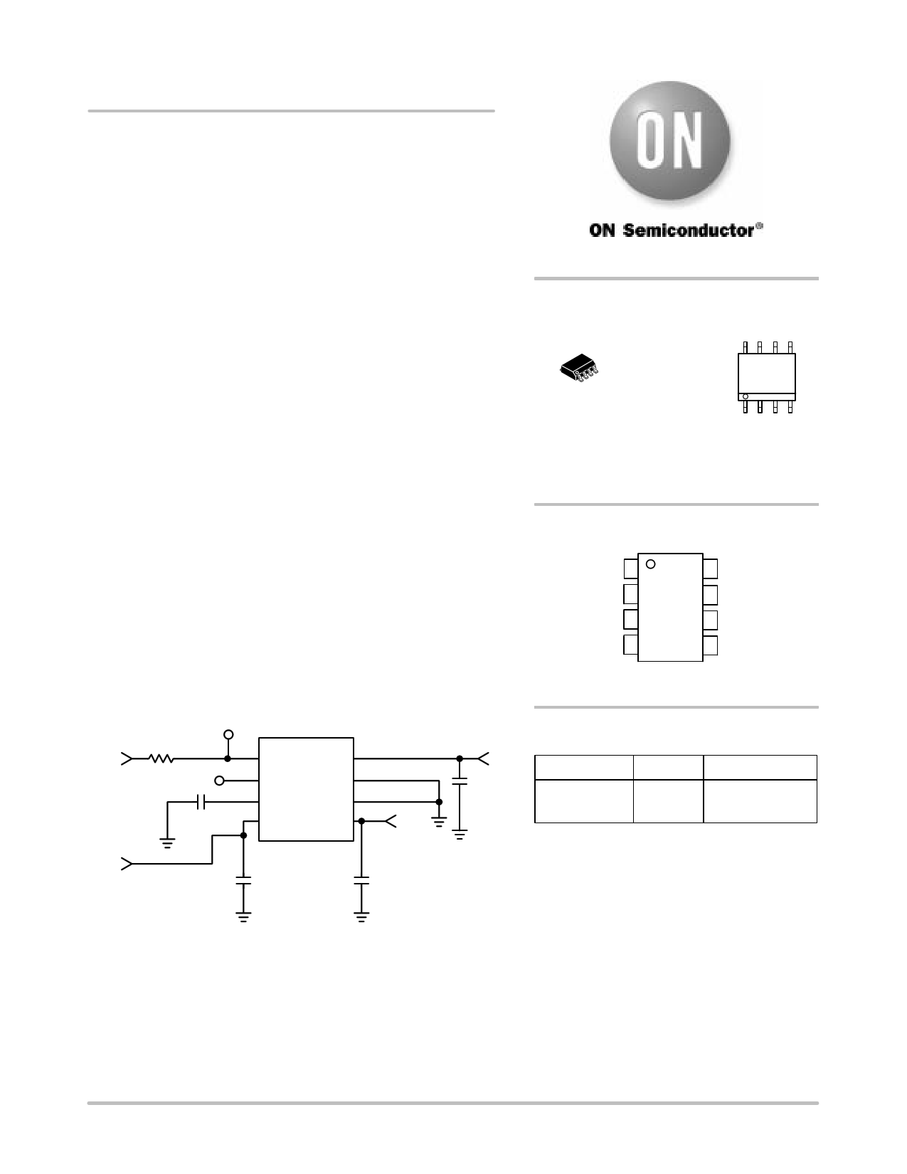
Vin RST
10 KW
Vin
Vin Rst Vout1
Vout Rst GND1
10 nF
CD GND2
Vin Vout2
Vout2
Vin Cin
0.1 mF
Cout2
4.7 mF
ORDERING INFORMATION
Vout1
Cout2
4.7 mF
Device
NCP4672DR2G
Package
SOIC−8
(Pb−Free)
Shipping†
2500 Tape & Reel
†For information on tape and reel specifications,
including part orientation and tape sizes, please
refer to our Tape and Reel Packaging Specifications
Brochure, BRD8011/D.
Figure 1. Typical Application Circuit
© Semiconductor Components Industries, LLC, 2004
February, 2004 − Rev. 4
1
Publication Order Number:
NCP4672/D
1 page 
VOPLin*
Vi
(Pin4)
VSHin
DVSin
NCP4672
VSLin
VOPLin*
Vin RST
(Pin1)
Vout1
(Pin8)
VOPLout*
VSHout
DVSout
VSLout
VOPLout*
Vo RST
(Pin2)
tPLH
tPHL
tPLH
*; VOPLin shows theoretical on this chart.
VOPLin spec. must be specified on Pin 1 voltage (0.4 V)
*; VOPLout shows theoretical on this chart.
VOPLout spec. must be specified on Pin 2 voltage (0.4 V)
Figure 2. Dual Regulator Timing
Vin 4 VOPLin = 1.0 Vtyp
GND1 7
+ 7.0 V
−
Vin RST
1
10 kW
VOLin = 0.4 V
+
− Vt1
Vtyp = 5.0 V
Vmax = 16 V
Figure 3. Threshold Operating Voltage VOPLin Under Condition VOLin = 0.4 V
http://onsemi.com
5
5 Page | ||
| Páginas | Total 8 Páginas | |
| PDF Descargar | [ Datasheet NCP4672.PDF ] | |
Hoja de datos destacado
| Número de pieza | Descripción | Fabricantes |
| NCP4671 | Dual Rail Ultra Low Dropout Linear Regulator | ON Semiconductor |
| NCP4672 | Dual Linear Voltage Regulators | ON Semiconductor |
| Número de pieza | Descripción | Fabricantes |
| SLA6805M | High Voltage 3 phase Motor Driver IC. |
Sanken |
| SDC1742 | 12- and 14-Bit Hybrid Synchro / Resolver-to-Digital Converters. |
Analog Devices |
|
DataSheet.es es una pagina web que funciona como un repositorio de manuales o hoja de datos de muchos de los productos más populares, |
| DataSheet.es | 2020 | Privacy Policy | Contacto | Buscar |