|
|
|
PDF NB3RL02 Data sheet ( Hoja de datos )
| Número de pieza | NB3RL02 | |
| Descripción | Low Phase-Noise Two-Channel Clock Fanout Buffer | |
| Fabricantes | ON Semiconductor | |
| Logotipo | ||
Hay una vista previa y un enlace de descarga de NB3RL02 (archivo pdf) en la parte inferior de esta página. Total 8 Páginas | ||
|
No Preview Available !
www.DataSheet.co.kr
NB3RL02
Low Phase-Noise
Two-Channel Clock Fanout
Buffer
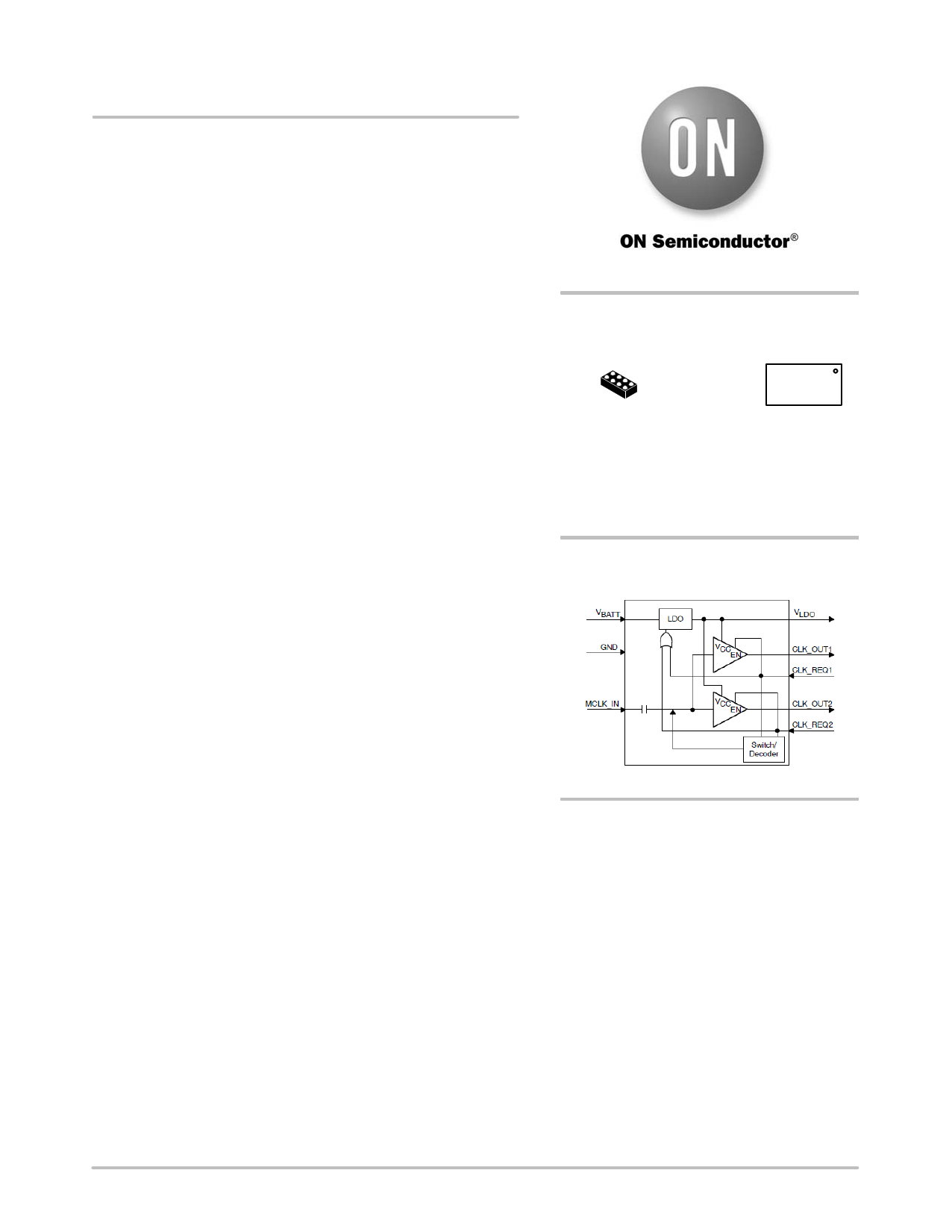
The NB3RL02 is a low−skew, low jitter 1:2 clock fan−out buffer,
ideal for use in portable end−equipment, such as mobile phones. With
integrated LDO and output control circuitry.
The MCLK_IN pin has an AC coupling capacitor and will directly
accept a square or sine wave clock input, such as a temperature
compensated crystal oscillator (TCXO). The minimum acceptable
input amplitude of the sine wave is 300 mV peak−to−peak.
The two clock outputs are enabled by control inputs CLK_REQ1
and CLK_REQ2.
The NB3RL02 has an integrated Low−Drop−Out (LDO) voltage
regulator which accepts input voltages from 2.3 V to 5.5 V and outputs
1.8 V at Iout = 50 mA. This 1.8 V supply is externally available to
provide regulated power to peripheral devices, such as a TCXO.
The adaptive clock output buffers offer controlled slew−rate over a
wide capacitive loading range which minimizes EMI emissions,
maintains signal integrity, and minimizes ringing caused by signal
reflections on the clock distribution lines.
The NB3RL02 is offered in a 0.4 mm pitch wafer−level−chip−scale
(WLCS) package (0.8 mm x 1.6 mm) and is optimized for very low
standby current consumption.
Features
• Low Additive Noise:
♦ −149 dBc/Hz at 10 kHz Offset Phase Noise
♦ 0.37 ps (rms) Output Jitter
• Limited Output Slew Rate for EMI Reduction
(1 ns to 5 ns/Rise/Fall Time for 10−50 pF Loads)
• Regulated 1.8 V Output Supply Available for External Clock Source,
ie. TCX0
• Ultra−Small Package:
♦ 8−ball: 0.4 mm Pitch WLCS (0.8 mm x 1.6 mm)
• ESD Performance Exceeds JESD 22
♦ 2000 V Human−Body Model (A114−A)
♦ 200 V Machine Model (A115−A)
♦ 1000 V Charged−Device Model (JESD22−C101−A Level III)
• These are Pb−Free Devices
Applications
• Cellular Phones
• Global Positioning Systems (GPS)
http://onsemi.com
MARKING
DIAGRAMS
WLCSP8
CASE 499BQ
RLYYWW
G
RL = Specific Device Code
YY = Year
WW = Work Week
G = Pb−Free Package
LOGIC DIAGRAM
ORDERING INFORMATION
See detailed ordering and shipping information in the package
dimensions section on page 7 of this data sheet.
© Semiconductor Components Industries, LLC, 2011
July, 2011 − Rev. 1
1
Publication Order Number:
NB3RL02/D
Datasheet pdf - http://www.DataSheet4U.net/
1 page 
www.DataSheet.co.kr
NB3RL02
Table 5. ELECTRICAL CHARACTERISTICS (TA = −40°C to +85°C)
Symbol
Parameter
Test Conditions
Min Typ Max Unit
MCLK_IN SINUSOIDAL SOURCE
VMA Input amplitude
Phase noise
fIN = 26 MHz,
VMA = 1.8 VPP
1 kHz offset
10 kHz offset
0.3 1.8 V
−138
dBc/Hz
−146
100 kHz offset
−151
1 MHz offset
−149
fIN = 26 MHz,
VMA = 0.8 VPP
1 kHz offset
10 kHz offset
−138
−146
100 kHz offset
−150
1 MHz offset
−148
Additive jitter
fIN = 26 MHz, VMA = 1.8 VPP,
BW = 10 kHz − 5 MHz
0.37 ps
(rms)
tDS MCLK_IN to CLK_OUT_1/2
propagation delay
12 ns
DC Output duty cycle
CLK_OUT_N OUTPUTS
fIN = 26 MHz, VMA > 1.8 VPP
45 50 55
%
tr 20% to 80% rise time
CL = 10 pF to 50 pF
1
5 ns
tf 20% to 80% fall time
CL = 10 pF to 50 pF
1
5 ns
tsk Channel−to−channel skew
CL = 10 pF to 50 pF, (CL1 = CL2)
−0.5
0.5 ns
VOH High−level output voltage
IOH = −100 mA, reference to VLDO
−0.1
V
IOH = −8 mA
1.2
VOL Low−level output voltage
IOL = 20 mA
0.2 V
IOL = 8 mA
0.45
NOTE: Device will meet the specifications after thermal equilibrium has been established when mounted in a test socket or printed
circuit board with maintained transverse airflow greater than 500 lfpm. Electrical parameters are guaranteed only over the
declared operating temperature range. Functional operation of the device exceeding these conditions is not implied. Device
specification limit values are applied individually under normal operating conditions and not valid simultaneously.
http://onsemi.com
5
Datasheet pdf - http://www.DataSheet4U.net/
5 Page | ||
| Páginas | Total 8 Páginas | |
| PDF Descargar | [ Datasheet NB3RL02.PDF ] | |
Hoja de datos destacado
| Número de pieza | Descripción | Fabricantes |
| NB3RL02 | Low Phase-Noise Two-Channel Clock Fanout Buffer | ON Semiconductor |
| Número de pieza | Descripción | Fabricantes |
| SLA6805M | High Voltage 3 phase Motor Driver IC. |
Sanken |
| SDC1742 | 12- and 14-Bit Hybrid Synchro / Resolver-to-Digital Converters. |
Analog Devices |
|
DataSheet.es es una pagina web que funciona como un repositorio de manuales o hoja de datos de muchos de los productos más populares, |
| DataSheet.es | 2020 | Privacy Policy | Contacto | Buscar |