|
|
|
PDF NCP703 Data sheet ( Hoja de datos )
| Número de pieza | NCP703 | |
| Descripción | LDO Voltage Regulator | |
| Fabricantes | ON Semiconductor | |
| Logotipo | ||
Hay una vista previa y un enlace de descarga de NCP703 (archivo pdf) en la parte inferior de esta página. Total 18 Páginas | ||
|
No Preview Available !
NCP703
300 mA, Ultra-Low Quiescent
Current, IQ 12 mA, Ultra-Low
Noise, LDO Voltage Regulator
Noise sensitive RF applications such as Power Amplifiers in
satellite radios, infotainment equipment, and precision
instrumentation require very clean power supplies. The NCP703 is
300 mA LDO that provides the engineer with a very stable, accurate
voltage with ultra low noise and very high Power Supply Rejection
Ratio (PSRR) suitable for RF applications. The device doesn’t require
any additional noise bypass capacitor to achieve ultra−low noise
performance. In order to optimize performance for battery operated
portable applications, the NCP703 employs dynamic Iq management
for ultra−low quiescent current consumption at light−load conditions
and great dynamic performance.
Features
• Operating Input Voltage Range: 2.0 V to 5.5 V
• Available in Fixed Voltage Options: 0.8 to 3.5 V
Contact Factory for Other Voltage Options
• Ultra−Low Quiescent Current of Typ. 12 mA
• Ultra−Low Noise: 13 mVRMS from 100 Hz to 100 kHz
• Very Low Dropout: 180 mV Typical at 300 mA
• ±2% Accuracy Over Load/Line/Temperature
• High PSRR: 68 dB at 1 kHz
• Internal Soft−Start to Limit the Turn−On Inrush Current
• Thermal Shutdown and Current Limit Protections
• Stable with a 1 mF Ceramic Output Capacitor
• Available in TSOP−5 and XDFN 1.5 x 1.5 mm Package
• Active Output Discharge for Fast Turn−Off
• These are Pb−Free Devices
Typical Applicaitons
• PDAs, Mobile Phones, GPS, Smartphones
• Wireless Handsets, Wireless LAN, Bluetooth, Zigbee
• Portable Medical Equipment
• Other Battery Powered Applications
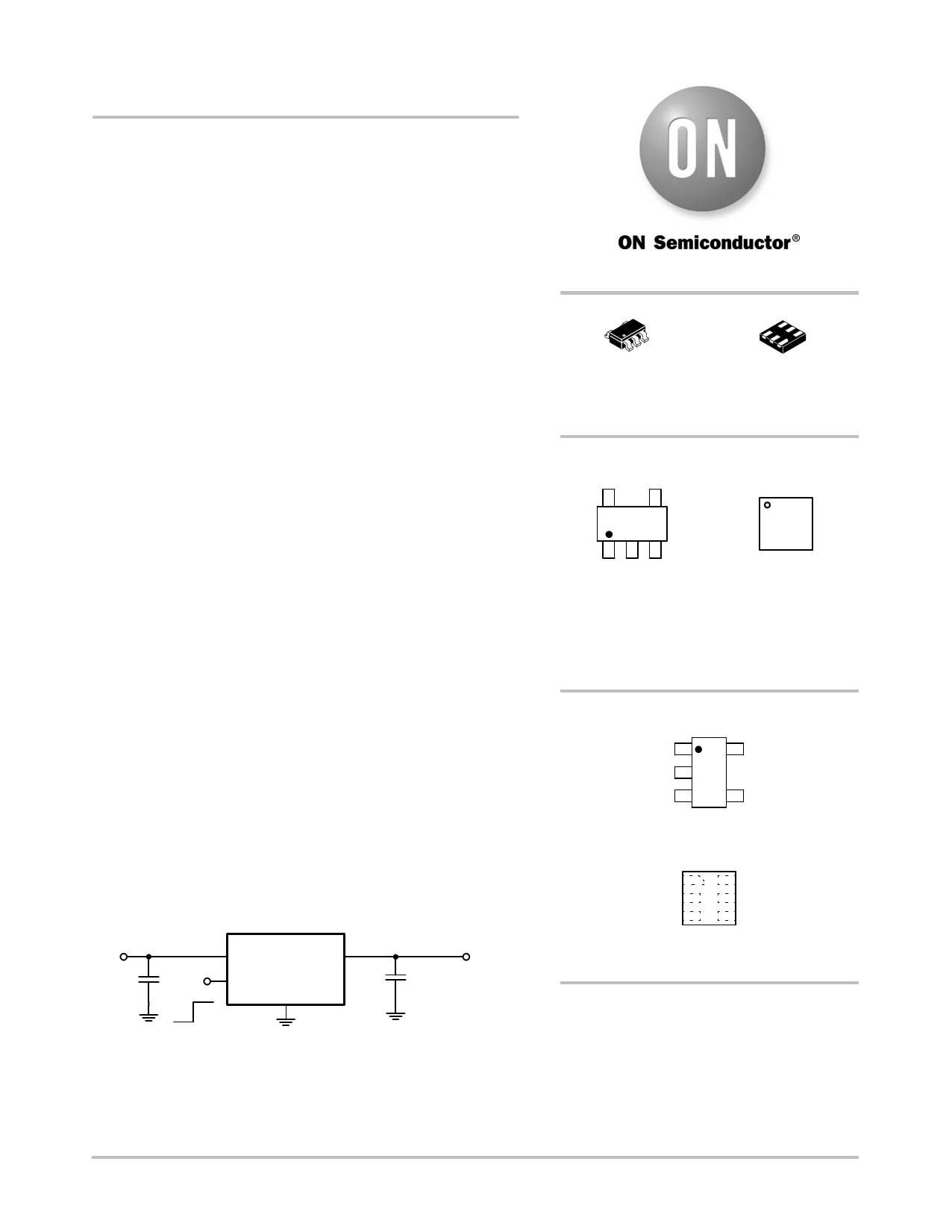
VIN
IN OUT
VOUT
CIN 1 mF
NCP703
EN
ON GND
COUT
1 mF
Ceramic
OFF
Figure 1. Typical Application Schematic
http://onsemi.com
5
1
TSOP−5
SN SUFFIX
CASE 483
1
XDFN6
MX SUFFIX
CASE 711AE
MARKING DIAGRAMS
5
XXXAYW
G
1
1
XM
G
X, XXX = Specific Device Code
M = Date Code
A = Assembly Location
Y = Year
W = Work Week
G = Pb−Free Package
PIN CONNECTIONS
1
IN OUT
GND
EN N/C
5−Pin TSOP−5
(Top View)
OUT
N/C
GND
1
IN
N/C
EN
6−Pin XDFN 1.5 x 1.5 mm
(Top View)
ORDERING INFORMATION
See detailed ordering and shipping information in the package
dimensions section on page 16 of this data sheet.
© Semiconductor Components Industries, LLC, 2012
September, 2012 − Rev. 0
1
Publication Order Number:
NCP703/D
Free Datasheet http://www.datasheet4u.com/
1 page 
NCP703
TYPICAL CHARACTERISTICS
10
1
0.1
0.01
VIN = 3.8 V
VOUT = 3.3 V
CIN = 1 mF
COUT = 4.7 mF
MLCC, X7R,
1206 size
0.001
0.01 0.1
IOUT = 300 mA
IOUT = 10 mA
IOUT = 1 mA
1 10 100 1000
IOUT
1 mA
10 mA
300 mA
RMS Output Noise (mV)
10 Hz − 100 kHz 100 Hz − 100 kHz
17.64
13.52
19.54
15.96
21.50
18.71
FREQUENCY (kHz)
Figure 6. Output Voltage Noise Spectral Density for VOUT = 3.3 V, COUT = 4.7 mF
350
315 VOUT = 0.8 V
280
245 VOUT = 3.3 V
210 VOUT = 2.5 V
175
140
105
70
35
0
0
VIN = VOUT + 0.5 V
CIN = 1 mF
COUT = 1 mF
MLCC, X7R,
1206 size
50 100 150 200 250 300
IOUT, OUTPUT CURRENT (mA)
Figure 7. Ground Current vs. Output Current
270
240
TJ = 25°C
TJ = 125°C
210
180 TJ = −40°C
150
120
90
60
30
0
0
30 60
VIN = VOUT + 0.5 V
CIN = 1 mF
COUT = 1 mF
MLCC, X7R,
1206 size
90 120 150 180 210 240 270 300
IOUT, OUTPUT CURRENT (mA)
Figure 9. Ground Current vs. Output Current
at Temperatures
160
140
VOUT = 3.3 V
120
VOUT = 2.5 V
100
VOUT = 0.8 V
80
60 VIN = VOUT + 0.5 V
CIN = 1 mF
40 COUT = 1 mF
MLCC, X7R,
20 1206 size
0
0 0.25 0.50 0.75 1.00 1.25 1.50 1.75 2.00
IOUT, OUTPUT CURRENT (mA)
Figure 8. Ground Current vs. Output Current
from 0 mA to 2 mA
160
140
120
100 TJ = −40°C
80
TJ = 25°C
TJ = 125°C
60
40
20
0
0
VIN = VOUT + 0.5 V
CIN = 1 mF
COUT = 1 mF
MLCC, X7R,
1206 size
0.25 0.50 0.75 1.00 1.25 1.50 1.75 2.00
IOUT, OUTPUT CURRENT (mA)
Figure 10. Ground Current vs. Output Current
0 mA to 2 mA at Temperatures
http://onsemi.com
5
5 Page 
NCP703
TYPICAL CHARACTERISTICS
IOUT
VIN = 2 V
VOUT = 0.8 V
CIN = 1 mF (MLCC)
IOUT
VIN = 2 V
VOUT = 0.8 V
CIN = 1 mF (MLCC)
VOUT
COUT = 4.7 mF
COUT = 1 mF
20 ms / div
Figure 41. Load Transient Response − Rising
Edge, VOUT = 0.8 V, IOUT = 1 mA to 300 mA,
COUT = 1 mF, 4.7 mF
VOUT
COUT = 1 mF
COUT = 4.7 mF
50 ms / div
Figure 42. Load Transient Response – Falling
Edge, VOUT = 0.8 V, IOUT = 1 mA to 300 mA,
COUT = 1 mF, 4.7 mF
IOUT
VIN = 2 V
VOUT = 0.8 V
CIN = 1 mF (MLCC)
Cout = 1 mF (MLCC)
VOUT
trise = 10 ms
trise = 1 ms
20 ms / div
Figure 43. Load Transient Response − Rising
Edge, VOUT = 0.8 V, IOUT = 1 mA to 300 mA,
tRISE = 1 ms, 10 ms
IOUT
VIN = 3.8 V
VOUT = 3.3 V
CIN = 1 mF (MLCC)
VOUT
COUT = 1 mF
COUT = 4.7 mF
50 ms / div
Figure 45. Load Transient Response – Falling
Edge, VOUT = 3.3 V, IOUT = 1 mA to 300 mA,
COUT = 1 mF, 4.7 mF
IOUT
VIN = 3.8 V
VOUT = 3.3 V
CIN = 1 mF (MLCC)
VOUT
COUT = 4.7 mF
COUT = 1 mF
10 ms / div
Figure 44. Load Transient Response – Rising
Edge, VOUT = 3.3 V, IOUT = 1 mA to 300 mA,
COUT = 1 mF, 4.7 mF
IOUT
VOUT
VIN = 3.8 V
VOUT = 3.3 V
CIN = 1 mF (MLCC)
Cout = 1 mF (MLCC)
trise = 1 ms
trise = 10 ms
10 ms / div
Figure 46. Load Transient Response – Rising
Edge, VOUT = 3.3 V, IOUT = 1 mA to 300 mA,
tRISE = 1 ms, 10 ms
http://onsemi.com
11
11 Page | ||
| Páginas | Total 18 Páginas | |
| PDF Descargar | [ Datasheet NCP703.PDF ] | |
Hoja de datos destacado
| Número de pieza | Descripción | Fabricantes |
| NCP700 | BiCMOS RF LDO Regulator | ON Semiconductor |
| NCP700B | BiCMOS RF LDO Regulator | ON Semiconductor |
| NCP700C | BiCMOS RF LDO Regulator | ON Semiconductor |
| NCP702 | LDO Linear Voltage Regulator | On Semiconductor |
| Número de pieza | Descripción | Fabricantes |
| SLA6805M | High Voltage 3 phase Motor Driver IC. |
Sanken |
| SDC1742 | 12- and 14-Bit Hybrid Synchro / Resolver-to-Digital Converters. |
Analog Devices |
|
DataSheet.es es una pagina web que funciona como un repositorio de manuales o hoja de datos de muchos de los productos más populares, |
| DataSheet.es | 2020 | Privacy Policy | Contacto | Buscar |