|
|
|
PDF NCP706 Data sheet ( Hoja de datos )
| Número de pieza | NCP706 | |
| Descripción | Very Low Dropout Voltage Regulator | |
| Fabricantes | ON Semiconductor | |
| Logotipo | ||
Hay una vista previa y un enlace de descarga de NCP706 (archivo pdf) en la parte inferior de esta página. Total 12 Páginas | ||
|
No Preview Available !
NCP706
1A, 1% Precision Very Low
Dropout Voltage Regulator
with Enable
The NCP706 is a Very Low Dropout Regulator which provides up to
1 A of load current and maintains excellent output voltage accuracy of
1% including line, load and temperature variations. The operating
input voltage range from 2.4 V up to 5.5 V makes this device suitable
for Li−ion battery powered products as well as post−regulation
applications. The product is available in 2.1 V and 2.2 V fixed output
voltage options. NCP706 is fully protected against overheating and
output short circuit.
Very small 8−pin XDFN8 1.6 x 1.2, 04P package makes the device
especially suitable for space constrained portable applications such as
tablets and smartphones.
Features
• Operating Input Voltage Range: 2.4 V to 5.5 V
• Fixed Output Voltage Option: 2.1 V, 2.2 V
Other Output Voltage Options available on request.
• Low Quiescent Current of typ. 200 mA
• Very Low Dropout: 300 mV Max. at IOUT = 1 A
• ±1% Accuracy Over Load/Line/Temperature
• High PSRR: 60 dB at 1 kHz
• Internal Soft−Start to Limit the Inrush Current
• Thermal Shutdown and Current Limit Protections
• Stable with a 4.7 mF Ceramic Output Capacitor
• Available in XDFN8 1.6 x 1.2, 04P 8−pin package
• These are Pb−Free Devices
Typical Applications
• Tablets, Smartphones,
• Wireless Handsets, Portable Media Players
• Portable Medical Equipment
• Other Battery Powered Applications
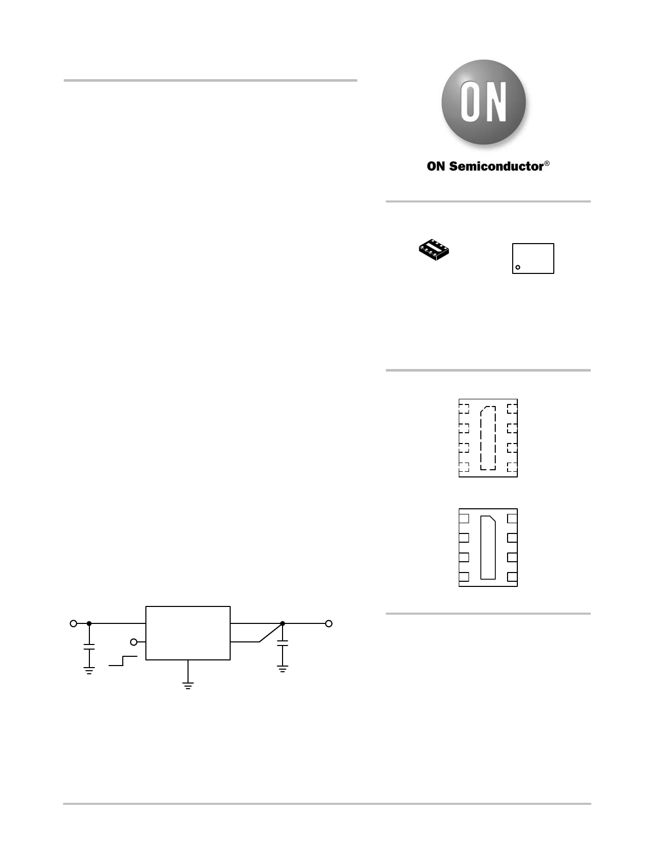
VIN = 2.4 (2.5) − 5.5 V
CIN
ON
OFF
IN
EN
NCP706
GND
OUT
SNS
VOUT = 2.1 (2.2) V @ 1 A
COUT
4.7 mF
Ceramic
http://onsemi.com
XDFN8
CASE 711AS
MARKING
DIAGRAM
XXMG
G
XX = Specific Device Code
M = Date Code
G = Pb−Free Package
(*Note: Microdot may be in either location)
PIN CONNECTION
OUT 1
8 IN
OUT 2
7 IN
N/C 3
6 EN
SNS 4
5 GND
(Top View)
IN 8
1 OUT
IN 7
2 OUT
EN 6
3 N/C
GND 5
4 SNS
(Bottom View)
ORDERING INFORMATION
See detailed ordering and shipping information on page 11 of
this data sheet.
Figure 1. Typical Application Schematic
© Semiconductor Components Industries, LLC, 2013
July, 2013 − Rev. 2
1
Publication Order Number:
NCP706/D
Free Datasheet http://www.datasheet4u.com/
1 page 
NCP706
ELECTRICAL CHARACTERISTICS − VOLTAGE VERSION 2.2 V
−40°C ≤ TJ ≤ 125°C; VIN = VOUT(NOM) + 0.3 V or 2.5 V, whichever is greater; IOUT = 10 mA, CIN = COUT = 4.7 mF, VEN = 0.9 V, unless
otherwise noted. Typical values are at TJ = +25°C. (Note 5)
Parameter
Test Conditions
Symbol Min Typ Max Unit
Operating Input Voltage
VIN 2.5
5.5 V
Undervoltage lock−out
Output Voltage Accuracy
Line Regulation
Load Regulation
Load Transient
Dropout voltage (Note 6)
Output Current Limit
Quiescent current
VIN rising
VOUT + 0.3 V ≤ VIN ≤ 4.5 V, IOUT = 0 – 1 A
VOUT + 0.3 V ≤ VIN ≤ 4.5 V, IOUT = 10 mA
IOUT = 0 mA to 1 A
IOUT = 10 mA to 1A or 10 mA to 1 A in 10 ms,
COUT = 10 mF
IOUT = 1 A, VOUT(nom) = 2.2 V
VOUT = 90% VOUT(nom)
IOUT = 0 mA
UVLO
VOUT
RegLINE
RegLOAD
TranLOAD
1.2
2.178
VDO
ICL
IQ
1.1
1.6
2.2
2
2
±120
180
1.9
2.222
300
230
V
V
mV
mV
mV
mV
A
mA
Ground current
IOUT = 1 A
IGND
200 mA
Shutdown current
VEN ≤ 0 V, VIN = 2.0 to 5.5 V
0.1 1 mA
EN Pin High Threshold
EN Pin Low Threshold
VEN Voltage increasing
VEN Voltage decreasing
VEN_HI
VEN_LO
0.9
V
0.4
EN Pin Input Current
VEN = 5.5 V
IEN
100 500
nA
Turn−on Time
COUT = 4.7 mF, from assertion EN pin to 98%
Vout(nom)
tON
200 ms
Power Supply Rejection Ratio
VIOINUT==30.2.5VA, VOUT = 2.2 V
f = 100 Hz
f = 1 kHz
PSRR
55
70
dB
f = 10 kHz
60
Output Noise Voltage
VOUT = 2.2 V, VIN = 2.7 V, IOUT = 0.5 A
f = 100 Hz to 100 kHz
VNOISE
300 mVrms
Thermal Shutdown Temperature Temperature increasing from TJ = +25°C
TSD
160 °C
Thermal Shutdown Hysteresis
Temperature falling from TSD
TSDH
− 20
− °C
5. Performance guaranteed over the indicated operating temperature range by design and/or characterization production tested at TJ = TA =
25_C. Low duty cycle pulse techniques are used during testing to maintain the junction temperature as close to ambient as possible.
6. Characterized when VOUT falls 100 mV below the regulated voltage at VIN = VOUT(NOM) + 0.3 V.
http://onsemi.com
5
5 Page 
NCP706
APPLICATIONS INFORMATION
Input Decoupling (Cin)
A 4.7 mF capacitor either ceramic or tantalum is
recommended and should be connected as close as possible
to the pins of NCP706 device. Higher values and lower ESR
will improve the overall line transient response.
Output Decoupling (Cout)
The minimum decoupling value is 4.7 mF and can be
augmented to fulfill stringent load transient requirements.
The regulator accepts ceramic chip capacitors MLCC. If a
tantalum capacitor is used, and its ESR is large, the loop
oscillation may result. Larger values improve noise
rejection and PSRR.
Enable Operation
The enable pin EN will turn on or off the regulator. These
limits of threshold are covered in the electrical specification
section of this data sheet. If the enable is not used then the
pin should be connected to VIN.
Hints
Please be sure the Vin and GND lines are sufficiently wide.
If their impedance is high, noise pickup or unstable
operation may result.
Set external components, especially the output capacitor,
as close as possible to the circuit.
The sense pin SNS trace is recommended to be kept as far
from noisy power traces as possible and as close to load as
possible.
Thermal
As power across the NCP706 increases, it might become
necessary to provide some thermal relief. The maximum
power dissipation supported by the device is dependent
upon board design and layout. Mounting pad configuration
on the PCB, the board material, and also the ambient
temperature affect the rate of temperature rise for the part.
This is stating that when the NCP706 has good thermal
conductivity through the PCB, the junction temperature will
be relatively low with high power dissipation.
The power dissipation across the device can be roughly
represented by the equation:
PD + ǒVIN * VOUTǓ * IOUT [W]
(eq. 1)
The maximum power dissipation depends on the thermal
resistance of the case and circuit board, the temperature
differential between the junction and ambient, PCB
orientation and the rate of air flow.
The maximum allowable power dissipation can be
calculated using the following equation:
PMAX + ǒTJ * TAǓńqJA [W]
(eq. 2)
Where (TJ − TA) is the temperature differential between
the junction and the surrounding environment and qJA is the
thermal resistance from the junction to the ambient.
Connecting the exposed pad and non connected pin 3 to
a large ground pad or plane helps to conduct away heat and
improves thermal relief.
ORDERING INFORMATION
Device
Nominal Ooutput
Voltage
Marking
Package
Shipping†
NCP706MX21TAG
2.1 V
QM XDFN8
(Pb−Free)
3000 / Tape & Reel
NCP706MX22TAG
2.2 V
QR XDFN8
(Pb−Free)
3000 / Tape & Reel
†For information on tape and reel specifications, including part orientation and tape sizes, please refer to our Tape and Reel Packaging
Specifications Brochure, BRD8011/D.
http://onsemi.com
11
11 Page | ||
| Páginas | Total 12 Páginas | |
| PDF Descargar | [ Datasheet NCP706.PDF ] | |
Hoja de datos destacado
| Número de pieza | Descripción | Fabricantes |
| NCP700 | BiCMOS RF LDO Regulator | ON Semiconductor |
| NCP700B | BiCMOS RF LDO Regulator | ON Semiconductor |
| NCP700C | BiCMOS RF LDO Regulator | ON Semiconductor |
| NCP702 | LDO Linear Voltage Regulator | On Semiconductor |
| Número de pieza | Descripción | Fabricantes |
| SLA6805M | High Voltage 3 phase Motor Driver IC. |
Sanken |
| SDC1742 | 12- and 14-Bit Hybrid Synchro / Resolver-to-Digital Converters. |
Analog Devices |
|
DataSheet.es es una pagina web que funciona como un repositorio de manuales o hoja de datos de muchos de los productos más populares, |
| DataSheet.es | 2020 | Privacy Policy | Contacto | Buscar |