|
|
PDF HIP6017 Data sheet ( Hoja de datos )
| Número de pieza | HIP6017 | |
| Descripción | Advanced PWM and Dual Linear Power Control | |
| Fabricantes | Intersil Corporation | |
| Logotipo |  |
|
Hay una vista previa y un enlace de descarga de HIP6017 (archivo pdf) en la parte inferior de esta página. Total 14 Páginas | ||
|
No Preview Available !
Data Sheet
HIP6017
April 1998 File Number 4496.1
Advanced PWM and Dual Linear Power
Control
The HIP6017 provides the power control and protection for
three output voltages in high-performance microprocessor
and computer applications. The IC integrates a PWM
controller, a linear regulator and a linear controller as well as
the monitoring and protection functions into a single 28 lead
SOIC package. The PWM controller regulates the
microprocessor core voltage with a synchronous-rectified
buck converter. The linear controller regulates power for the
GTL bus and the linear regulator provides power for the
clock driver circuits.
The HIP6017 includes an Intel-compatible, TTL 5-input
digital-to-analog converter (DAC) that adjusts the core PWM
output voltage from 2.1VDC to 3.5VDC in 0.1V increments
and from 1.8VDC to 2.05VDC in 0.05V steps. The precision
reference and voltage-mode control provide ±1% static
regulation. The linear regulator uses an internal pass device
to provide 2.5V ±2.5%. The linear controller drives an
external N-Channel MOSFET to provide 1.5V ±2.5%.
The HIP6017 monitors all the output voltages. A single
Power Good signal is issued when the core is within ±10% of
the DAC setting and the other levels are above their under-
voltage levels. Additional built-in over-voltage protection for
the core output uses the lower MOSFET to prevent output
voltages above 115% of the DAC setting. The PWM over-
current function monitors the output current by using the
voltage drop across the upper MOSFET’s rDS(ON), thus
eliminating the need for a current sensing resistor.
Pinout
HIP6017 (SOIC)
TOP VIEW
NC 1
NC 2
VID4 3
VID3 4
VID2 5
VID1 6
VID0 7
PGOOD 8
GND2 9
V33 10
NC 11
SS 12
FAULT/RT 13
FB2 14
28 VCC
27 UGATE1
26 PHASE1
25 LGATE1
24 PGND
23 OCSET1
22 VSEN1
21 FB1
20 COMP1
19 FB3
18 GATE3
17 GND
16 VOUT2
15 VIN2
Features
• Provides 3 Regulated Voltages
- Microprocessor Core, Clock and GTL Power
• Drives N-Channel MOSFETs
• Operates from +3.3V, +5V and +12V Inputs
• Simple Single-Loop PWM Control Design
- Voltage-Mode Control
• Fast Transient Response
- High-Bandwidth Error Amplifier
- Full 0% to 100% Duty Ratios
• Excellent Output Voltage Regulation
- Core PWM Output: ±1% Over Temperature
- Other Outputs: ±2.5% Over Temperature
• TTL-Compatible 5-Bit Digital-to-Analog Core Output
Voltage Selection
- Wide Range . . . . . . . . . . . . . . . . . . . 1.8VDC to 3.5VDC
- 0.1V Steps . . . . . . . . . . . . . . . . . . . . 2.1VDC to 3.5VDC
- 0.05V Steps . . . . . . . . . . . . . . . . . . 1.8VDC to 2.05VDC
• Power-Good Output Voltage Monitor
• Microprocessor Core Voltage Protection Against Shorted
MOSFET
• Over-Voltage and Over-Current Fault Monitors
- Does Not Require Extra Current Sensing Element,
Uses MOSFET’s rDS(ON)
• Small Converter Size
- Constant Frequency Operation
- 200kHz Free-Running Oscillator; Programmable from
50kHz to over 1MHz
Applications
• Full Motherboard Power Regulation for Computers
• Low-Voltage Distributed Power Supplies
Ordering Information
TEMP. RANGE
PART NUMBER
(oC)
PACKAGE PKG. NO.
HIP6017CB
0 to 70
28 Ld SOIC M28.3
HIP6017EVAL1 Evaluation Board
2-210
CAUTION: These devices are sensitive to electrostatic discharge; follow proper IC Handling Procedures.
http://www.intersil.com or 407-727-9207 | Copyright © Intersil Corporation 1999
1 page 
HIP6017
Electrical Specifications Recommended Operating Conditions, Unless Otherwise Noted. Refer to Figures 1, 2 and 3 (Continued)
PARAMETER
SYMBOL
TEST CONDITIONS
MIN TYP MAX UNITS
Slew Rate
SR COMP = 10pF
- 6 - V/µs
PWM CONTROLLER GATE DRIVER
Upper Drive Source
Upper Drive Sink
Lower Drive Source
Lower Drive Sink
PROTECTION
IUGATE
RUGATE
ILGATE
RLGATE
VCC = 12V, VUGATE1 = 6V
VUGATE1-PHASE1 = 1V
VCC = 12V, VLGATE1 = 1V
VLGATE1 = 1V
-1-
- 1.7 3.5
-1-
- 1.4 3.0
A
Ω
A
Ω
VOUT1 Over-Voltage Trip
FAULT Sourcing Current
OCSET1 Current Source
Soft-Start Current
Chip Shutdown Soft-Start Threshold
IOVP
IOCSET
ISS
VSEN1 Rising
VFAULT/RT = 10V
VOCSET = 4.5VDC
112 115 118
10 14
-
170 200 230
- 11 -
- - 1.0
%
mA
µA
µA
V
POWER GOOD
VOUT1 Upper Threshold
VOUT1 Under-Voltage (Lower Threshold)
VOUT1 Hysteresis (VSEN1/DACOUT)
PGOOD Voltage Low
VSEN1 Rising
VSEN1 Rising
Upper/Lower Threshold
VPGOOD IPGOOD = -4mA
108 - 110
92 - 94
-2-
- - 0.5
%
%
%
V
Typical Performance Curves
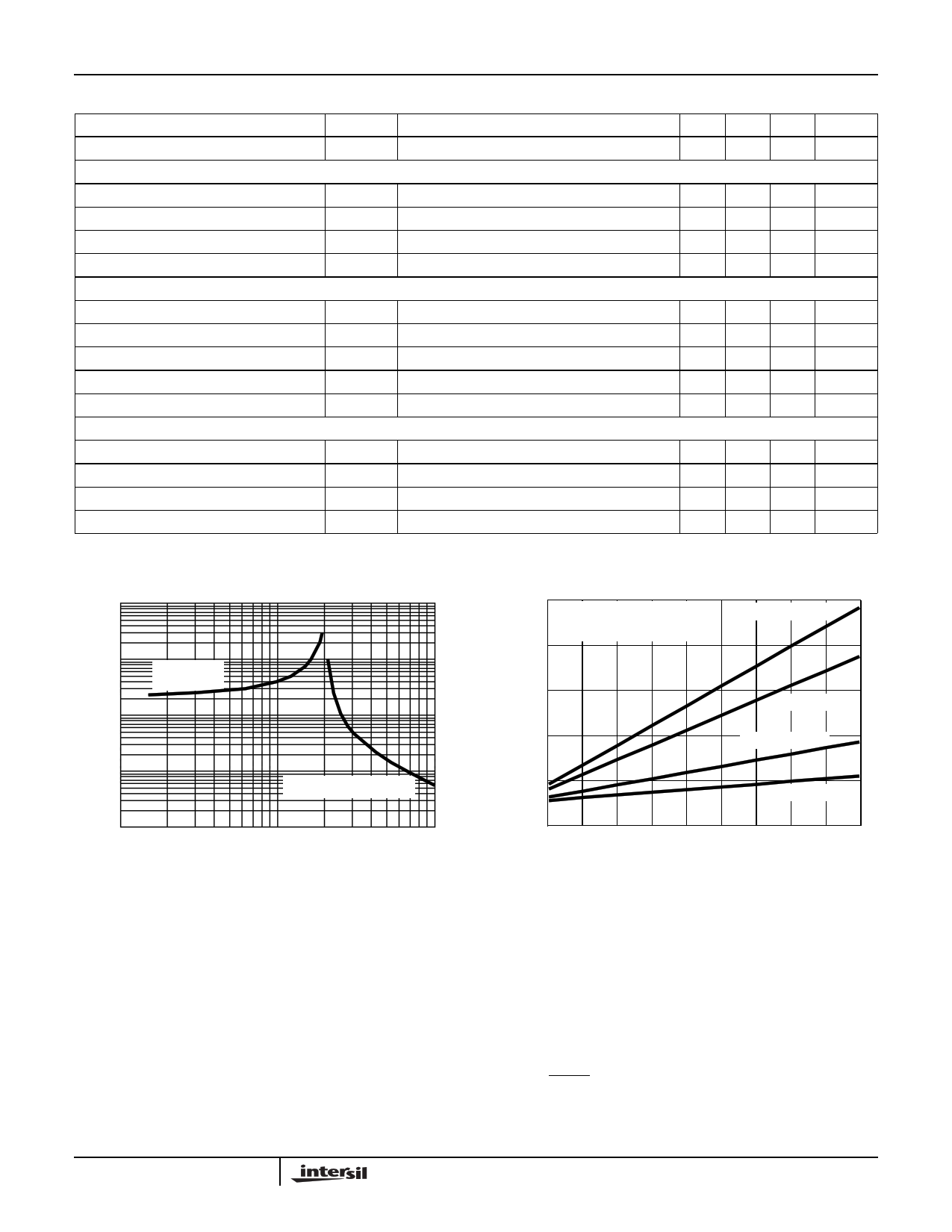
1000
100
RT PULLUP
TO +12V
10
RT PULLDOWN TO VSS
10 100
SWITCHING FREQUENCY (kHz)
FIGURE 4. RT RESISTANCE vs FREQUENCY
1000
Functional Pin Descriptions
VSEN1 (Pin 22)
This pin is connected to the PWM converter’s output voltage.
The PGOOD and OVP comparator circuits use this signal to
report output voltage status and for over-voltage protection.
OCSET1 (Pin 23)
Connect a resistor (ROCSET) from this pin to the drain of the
respective upper MOSFET. ROCSET, an internal 200µA
current source (IOCSET), and the upper MOSFET on-
100
CUGATE1 = CLGATE1 = CGATE
VVCC = 12V, VIN = 5V
80
CGATE = 4800pF
60
CGATE = 3600pF
40 CGATE = 1500pF
20
CGATE = 660pF
0
100 200
300 400 500 600 700 800
SWITCHING FREQUENCY (kHz)
900 1000
FIGURE 5. BIAS SUPPLY CURRENT vs FREQUENCY
resistance (rDS(ON)) set the converter over-current (OC) trip
point according to the following equation:
IPEAK
=
I--O-----C----S----E----T----x---R-----O----C----S----E----T--
rDS(ON)
An over-current trip cycles the soft-start function. Sustaining
an over-current for 2 soft-start intervals shuts down the IC.
Additionally, OCSET1 is an output for the inverted FAULT
signal (FAULT). If a fault condition causes FAULT to go high,
OCSET1 will be simultaneously pulled to ground though an
internal MOS device (typical rDS(ON) = 100Ω).
2-214
5 Page 
HIP6017
The modulator transfer function is the small-signal transfer
function of VOUT/VE/A. This function is dominated by a DC
gain and the output filter, with a double pole break frequency
at FLC and a zero at FESR. The DC gain of the modulator is
simply the input voltage, VIN, divided by the peak-to-peak
oscillator voltage, ∆VOSC.
Modulator Break Frequency Equations
FLC=
-------------------1--------------------
2π × LO × CO
FESR= 2----π-----×-----E----S--1---R------×-----C----O---
The compensation network consists of the error amplifier
internal to the HIP6017 and the impedance networks ZIN
and ZFB. The goal of the compensation network is to
provide a closed loop transfer function with an acceptable
0dB crossing frequency (f0dB) and adequate phase margin.
Phase margin is the difference between the closed loop
phase at f0dB and 180 degrees. The equations below relate
the compensation network’s poles, zeros and gain to the
components (R1, R2, R3, C1, C2, and C3) in Figure 11.
Use these guidelines for locating the poles and zeros of the
compensation network:
1. Pick Gain (R2/R1) for desired converter bandwidth
2. Place 1ST Zero Below Filter’s Double Pole (~75% FLC)
3. Place 2ND Zero at Filter’s Double Pole
4. Place 1ST Pole at the ESR Zero
5. Place 2ND Pole at Half the Switching Frequency
6. Check Gain against Error Amplifier’s Open-Loop Gain
7. Estimate Phase Margin - Repeat if Necessary
Compensation Break Frequency Equations
FZ1 = -2---π-----×-----R---1--2-----×----C-----1--
FZ2 = 2----π-----×-----(--R-----1-----+-1----R-----3----)---×-----C-----3-
FP1
=
---------------------------1---------------------------
2
π
×
R2
×
C-C----11-----+×-----CC-----22--
FP2 = -2---π-----×-----R---1--3-----×----C-----3--
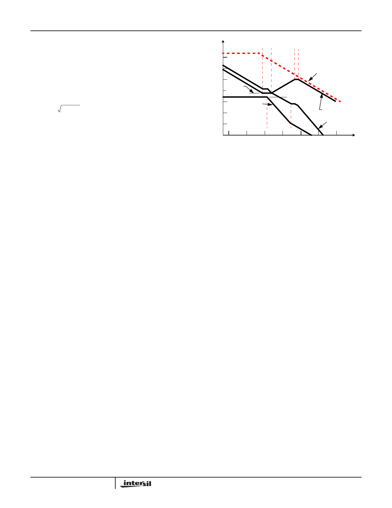
Figure 12 shows an asymptotic plot of the DC-DC
converter’s gain vs frequency. The actual modulator gain has
a peak due to the high Q factor of the output filter at FLC,
which is not shown in Figure 12. Using the above guidelines
should yield a compensation gain similar to the curve
plotted. The open loop error amplifier gain bounds the
compensation gain. Check the compensation gain at FP2
with the capabilities of the error amplifier. The closed loop
gain is constructed on the log-log graph of Figure 12 by
adding the modulator gain (in dB) to the compensation gain
(in dB). This is equivalent to multiplying the modulator
transfer function to the compensation transfer function and
plotting the gain.
100 FZ1 FZ2 FP1 FP2
80
OPEN LOOP
60 ERROR AMP GAIN
40
20LOG
20 (R2/R1)
0 MODULATOR
-20 GAIN
20LOG
(VIN/∆VOSC)
COMPENSATION
GAIN
-40
FLC FESR
CLOSED LOOP
GAIN
-60
10 100 1K 10K 100K 1M 10M
FREQUENCY (Hz)
FIGURE 12. ASYMPTOTIC BODE PLOT OF CONVERTER GAIN
The compensation gain uses external impedance networks
ZFB and ZIN to provide a stable, high bandwidth loop. A
stable control loop has a 0dB gain crossing with
-20dB/decade slope and a phase margin greater than 45
degrees. Include worst case component variations when
determining phase margin.
Component Selection Guidelines
Output Capacitor Selection
The output capacitors for each output have unique
requirements. In general the output capacitors should be
selected to meet the dynamic regulation requirements.
Additionally, the PWM converters require an output capacitor
to filter the current ripple. The linear regulator is internally
compensated and requires an output capacitor that meets
the stability requirements. The load transient for the
microprocessor core requires high quality capacitors to
supply the high slew rate (di/dt) current demands.
PWM Output Capacitors
Modern microprocessors produce transient load rates above
10A/ns. High frequency capacitors initially supply the
transient and slow the current load rate seen by the bulk
capacitors. The bulk filter capacitor values are generally
determined by the ESR (effective series resistance) and ESL
(effective series inductance) parameters rather than actual
capacitance.
High frequency decoupling capacitors should be placed as
close to the power pins of the load as physically possible. Be
careful not to add inductance in the circuit board wiring that
could cancel the usefulness of these low inductance
components. Consult with the manufacturer of the load on
specific decoupling requirements.
Use only specialized low-ESR capacitors intended for
switching regulator applications for the bulk capacitors. The
bulk capacitor’s ESR determines the output ripple voltage
and the initial voltage drop after a high slew-rate transient.
An aluminum electrolytic capacitor’s ESR value is related to
2-220
11 Page | ||
| Páginas | Total 14 Páginas | |
| PDF Descargar | [ Datasheet HIP6017.PDF ] | |
Hoja de datos destacado
| Número de pieza | Descripción | Fabricantes |
| HIP6011 | Buck Pulse-Width Modulator (PWM) Controller and Output Voltage Monitor | Intersil Corporation |
| HIP6012 | Buck and Synchronous-Rectifier Pulse-Width Modulator (PWM) Controller | Intersil Corporation |
| HIP6013 | Buck Pulse-Width Modulator (PWM) Controller | Intersil Corporation |
| HIP6014 | Buck and Synchronous-Rectifier (PWM) Controller and Output Voltage Monitor | Intersil Corporation |
| Número de pieza | Descripción | Fabricantes |
| SLA6805M | High Voltage 3 phase Motor Driver IC. |
Sanken |
| SDC1742 | 12- and 14-Bit Hybrid Synchro / Resolver-to-Digital Converters. |
Analog Devices |
|
DataSheet.es es una pagina web que funciona como un repositorio de manuales o hoja de datos de muchos de los productos más populares, |
| DataSheet.es | 2020 | Privacy Policy | Contacto | Buscar |
