|
|
|
PDF NTTFS4929N Data sheet ( Hoja de datos )
| Número de pieza | NTTFS4929N | |
| Descripción | Power MOSFET ( Transistor ) | |
| Fabricantes | ON Semiconductor | |
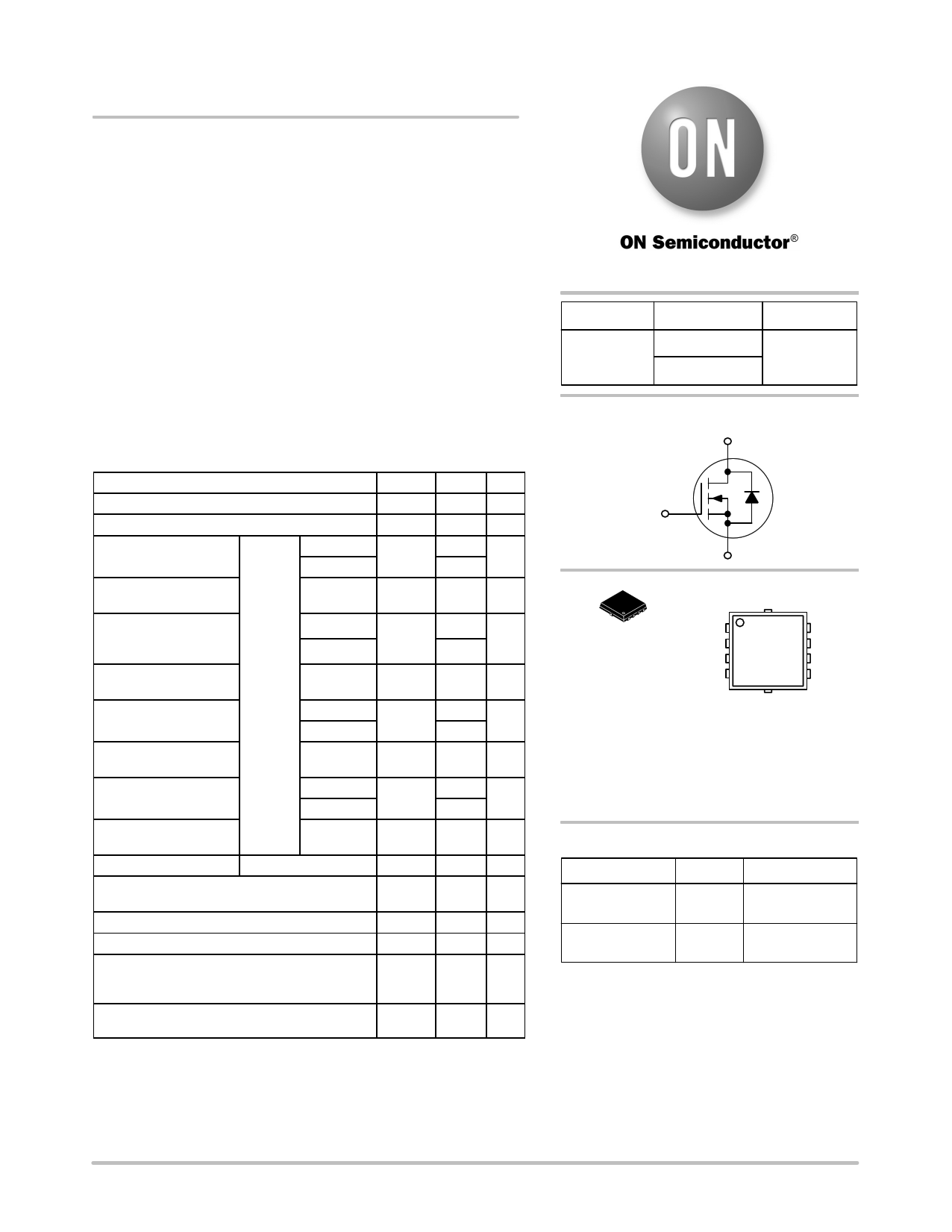
| Logotipo | ||
Hay una vista previa y un enlace de descarga de NTTFS4929N (archivo pdf) en la parte inferior de esta página. Total 7 Páginas | ||
|
No Preview Available !
NTTFS4929N
Power MOSFET
30 V, 34 A, Single N−Channel, m8FL
Features
• Low RDS(on) to Minimize Conduction Losses
• Low Capacitance to Minimize Driver Losses
• Optimized Gate Charge to Minimize Switching Losses
• These Devices are Pb−Free, Halogen Free/BFR Free and are RoHS
Compliant
Applications
• DC−DC Converters
• Power Load Switch
• Notebook Battery Management
• Motor Control
MAXIMUM RATINGS (TJ = 25°C unless otherwise stated)
Parameter
Symbol Value Unit
Drain−to−Source Voltage
Gate−to−Source Voltage
Continuous Drain
Current RqJA (Note 1)
Power Dissipation
(Note 1)
RqJA
TA = 25°C
TA = 85°C
TA = 25°C
VDSS
VGS
ID
PD
30
±20
10.6
7.7
2.11
V
V
A
W
Continuous Drain
C(Nuortreen1t)RqJA ≤ 10 s
TA = 25°C ID 14.3 A
TA = 85°C
10.3
Power Dissipation
RqJA ≤ 10 s (Note 1)
Continuous Drain
Current RqJA (Note 2)
Steady
State
TA = 25°C
TA = 25°C
TA = 85°C
Power Dissipation
RqJA (Note 2)
TA = 25°C
Continuous Drain
Current RqJC (Note 1)
TC = 25°C
TC = 85°C
Power Dissipation
RqJC (Note 1)
TC = 25°C
Pulsed Drain Current
TA = 25°C, tp = 10 ms
Operating Junction and Storage Temperature
Source Current (Body Diode)
Drain to Source dV/dt
PD 3.83 W
ID 6.6 A
4.7
PD 0.81 W
ID 34 A
25
PD 22.3 W
IDM
TTsJtg,
IS
dV/dt
115
−55 to
+150
22
6.0
A
°C
A
V/ns
Single Pulse Drain−to−Source Avalanche Energy EAS 16.2 mJ
(TJ = 25°C, VDD = 50 V, VGS = 10 V,
IL = 18 Apk, L = 0.1 mH, RG = 25 W)
Lead Temperature for Soldering Purposes
(1/8″ from case for 10 s)
TL 260 °C
Stresses exceeding Maximum Ratings may damage the device. Maximum
Ratings are stress ratings only. Functional operation above the Recommended
Operating Conditions is not implied. Extended exposure to stresses above the
Recommended Operating Conditions may affect device reliability.
1. Surface−mounted on FR4 board using 1 sq−in pad, 1 oz Cu.
2. Surface−mounted on FR4 board using the minimum recommended pad size.
http://onsemi.com
V(BR)DSS
30 V
RDS(on) MAX
11 mW @ 10 V
17 mW @ 4.5 V
ID MAX
34 A
N−Channel MOSFET
D (5−8)
G (4)
1
WDFN8
(m8FL)
CASE 511AB
S (1,2,3)
MARKING DIAGRAM
1
SD
S 4929 D
S AYWWG D
GGD
4929
A
Y
WW
G
= Specific Device Code
= Assembly Location
= Year
= Work Week
= Pb−Free Package
(Note: Microdot may be in either location)
ORDERING INFORMATION
Device
Package
Shipping†
NTTFS4929NTAG WDFN8 1500/Tape & Reel
(Pb−Free)
NTTFS4929NTWG WDFN8 5000/Tape & Reel
(Pb−Free)
†For information on tape and reel specifications,
including part orientation and tape sizes, please
refer to our Tape and Reel Packaging Specification
Brochure, BRD8011/D.
© Semiconductor Components Industries, LLC, 2011
May, 2011 − Rev. 0
1
Publication Order Number:
NTTFS4929N/D
Free Datasheet http://www.datasheet4u.com/
1 page 
NTTFS4929N
TYPICAL CHARACTERISTICS
1.7
1.6
1.5
ID = 20 A
VGS = 10 V
1.4
1.3
1.2
1.1
1
0.9
0.8
0.7
0.6
−50 −25
0
25 50 75 100 125
TJ, JUNCTION TEMPERATURE (°C)
Figure 5. On−Resistance Variation with
Temperature
1.0E−04
VGS = 0 V
1.0E−05
1.0E−06
1.0E−07
TJ = 150°C
TJ = 125°C
1.0E−08
1.0E−09
1.0E−10
TJ = 25°C
1.0E−11
150 10 15 20
VDS, DRAIN−TO−SOURCE VOLTAGE (V)
Figure 6. Drain−to−Source Leakage Current
vs. Voltage
25
1400
1200
1000
800
600
400
200
0
0
TJ = 25°C
Ciss VGS = 0 V
Coss
Crss
5 10 15 20 25
VDS, DRAIN−TO−SOURCE VOLTAGE (V)
Figure 7. Capacitance Variation
30
11
10
9
8
7
6
5
4 Qgs
3
2
1
0
02
QT
Qgd
468
TJ = 25°C
VGS = 10 V
VDD = 15 V
ID = 20 A
10 12 14 16
Qg, TOTAL GATE CHARGE (nC)
Figure 8. Gate−to−Source and
Drain−to−Source Voltage vs. Total Charge
1000
100
VGS = 10 V
VDD = 4.5 V
ID = 15 A
10
td(off)
tf
tr
td(on)
30
25
VGS = 0 V
TJ = 25°C
20
15
10
5
1
1 10 100
RG, GATE RESISTANCE (W)
Figure 9. Resistive Switching Time Variation
vs. Gate Resistance
0
0.1 0.2 0.3 0.4 0.5 0.6 0.7 0.8 0.9 1.0 1.1
VSD, SOURCE−TO−DRAIN VOLTAGE (V)
Figure 10. Diode Forward Voltage vs. Current
http://onsemi.com
5
Free Datasheet http://www.datasheet4u.com/
5 Page | ||
| Páginas | Total 7 Páginas | |
| PDF Descargar | [ Datasheet NTTFS4929N.PDF ] | |
Hoja de datos destacado
| Número de pieza | Descripción | Fabricantes |
| NTTFS4929N | Power MOSFET ( Transistor ) | ON Semiconductor |
| Número de pieza | Descripción | Fabricantes |
| SLA6805M | High Voltage 3 phase Motor Driver IC. |
Sanken |
| SDC1742 | 12- and 14-Bit Hybrid Synchro / Resolver-to-Digital Converters. |
Analog Devices |
|
DataSheet.es es una pagina web que funciona como un repositorio de manuales o hoja de datos de muchos de los productos más populares, |
| DataSheet.es | 2020 | Privacy Policy | Contacto | Buscar |