NTTFS4930N Datasheet PDF - ON Semiconductor
| Part Number | NTTFS4930N | |
| Description | Power MOSFET ( Transistor ) | |
| Manufacturers | ON Semiconductor | |
| Logo | ||
|
There is a preview and NTTFS4930N download ( pdf file ) link at the bottom of this page. Total 7 Pages | ||
Preview 1 page No Preview Available !
NTTFS4930N
Power MOSFET
30 V, 23 A, Single N−Channel, m8FL
Features
• Low RDS(on) to Minimize Conduction Losses
• Low Capacitance to Minimize Driver Losses
• Optimized Gate Charge to Minimize Switching Losses
• These Devices are Pb−Free, Halogen Free/BFR Free and are RoHS
Compliant
Applications
• DC−DC Converters
• Power Load Switch
• Notebook Battery Management
• Motor Control
MAXIMUM RATINGS (TJ = 25°C unless otherwise stated)
Parameter
Symbol
Drain−to−Source Voltage
VDSS
Gate−to−Source Voltage
Continuous Drain
Current RqJA (Note 1)
TA = 25°C
TA = 85°C
VGS
ID
Power Dissipation
(Note 1)
RqJA
TA = 25°C
PD
Value
30
±20
7.2
5.2
2.06
Unit
V
V
A
W
Continuous Drain
C(Nuortreen1t)RqJA ≤ 10 s
TA = 25°C
TA = 85°C
ID
9.6 A
6.9
Power Dissipation
RqJA ≤ 10 s (Note 1)
Continuous Drain
Current RqJA (Note 2)
Steady
State
TA = 25°C
TA = 25°C
TA = 85°C
Power Dissipation
RqJA (Note 2)
TA = 25°C
Continuous Drain
Current RqJC (Note 1)
TC = 25°C
TC = 85°C
Power Dissipation
RqJC (Note 1)
TC = 25°C
Pulsed Drain Current
TA = 25°C, tp = 10 ms
Operating Junction and Storage Temperature
Source Current (Body Diode)
Drain to Source dV/dt
PD 3.61 W
ID 4.5 A
3.2
PD 0.79 W
ID 23 A
16
PD 20.2 W
IDM
TJ,
Tstg
IS
dV/dt
92
−55 to
+150
25
6.0
A
°C
A
V/ns
Single Pulse Drain−to−Source Avalanche Energy
(TJ = 25°C, VDD = 50 V, VGS = 10 V,
IL = 12 Apk, L = 0.1 mH, RG = 25 W)
EAS
7.2 mJ
Lead Temperature for Soldering Purposes
(1/8″ from case for 10 s)
TL 260 °C
Stresses exceeding Maximum Ratings may damage the device. Maximum
Ratings are stress ratings only. Functional operation above the Recommended
Operating Conditions is not implied. Extended exposure to stresses above the
Recommended Operating Conditions may affect device reliability.
1. Surface−mounted on FR4 board using 1 sq−in pad, 1 oz Cu.
2. Surface−mounted on FR4 board using the minimum recommended pad size.
http://onsemi.com
V(BR)DSS
30 V
RDS(on) MAX
23 mW @ 10 V
30 mW @ 4.5 V
ID MAX
23 A
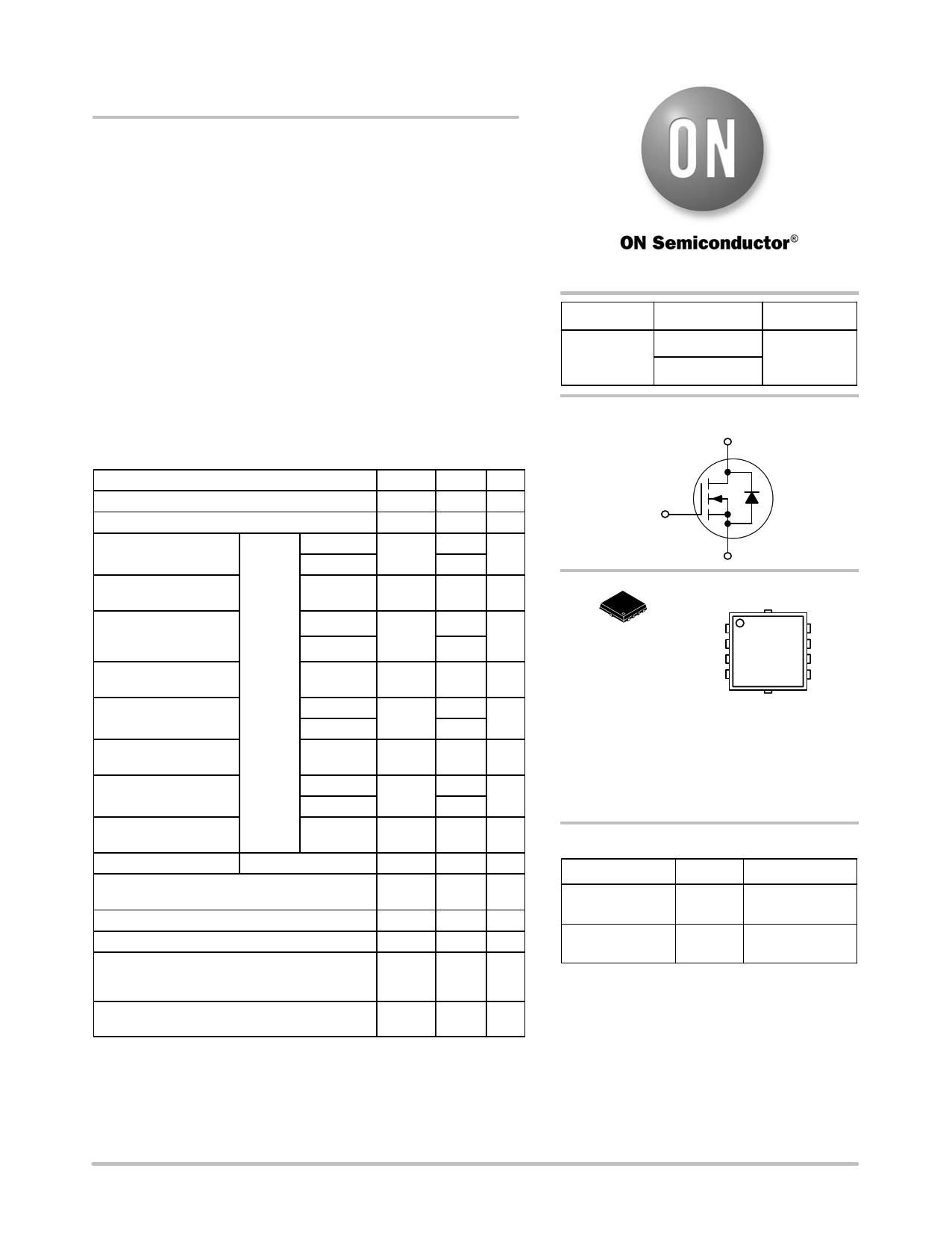
N−Channel MOSFET
D (5−8)
G (4)
1
WDFN8
(m8FL)
CASE 511AB
S (1,2,3)
MARKING DIAGRAM
1
SD
S 4930 D
S AYWWG D
GGD
4930
A
Y
WW
G
= Specific Device Code
= Assembly Location
= Year
= Work Week
= Pb−Free Package
(Note: Microdot may be in either location)
ORDERING INFORMATION
Device
Package
Shipping†
NTTFS4930NTAG WDFN8 1500/Tape & Reel
(Pb−Free)
NTTFS4930NTWG WDFN8 5000/Tape & Reel
(Pb−Free)
†For information on tape and reel specifications,
including part orientation and tape sizes, please
refer to our Tape and Reel Packaging Specification
Brochure, BRD8011/D.
© Semiconductor Components Industries, LLC, 2011
April, 2011 − Rev. 0
1
Publication Order Number:
NTTFS4930N/D
Free Datasheet http://www.datasheet4u.com/
|
| |

NTTFS4930N
TYPICAL CHARACTERISTICS
1.7
1.6 ID = 10 A
1.5 VGS = 10 V
1.4
1.3
1.2
1.1
1
0.9
0.8
0.7
0.6
−50 −25
0
25 50 75 100 125
TJ, JUNCTION TEMPERATURE (°C)
Figure 5. On−Resistance Variation with
Temperature
800
600 Ciss
TJ = 25°C
VGS = 0 V
400 Coss
200 Crss
0
0 5 10 15 20 25
VDS, DRAIN−TO−SOURCE VOLTAGE (V)
Figure 7. Capacitance Variation
1.0E−04
1.0E−05
VGS = 0 V
1.0E−06
1.0E−07
TJ = 150°C
TJ = 125°C
1.0E−08
1.0E−09
1.0E−10
TJ = 25°C
1501.0E−1110 15 20 25
VDS, DRAIN−TO−SOURCE VOLTAGE (V)
Figure 6. Drain−to−Source Leakage Current
vs. Voltage
30
11
10 QT
9
8
7
6
5
4 Qgs
Qgd
3
2
1
0
30 0 2 4
TJ = 25°C
VGS = 10 V
VDD = 15 V
ID = 20 A
6 8 10
Qg, TOTAL GATE CHARGE (nC)
Figure 8. Gate−to−Source and
Drain−to−Source Voltage vs. Total Charge
1000
VGS = 10 V
VDD = 15 V
100 ID = 15 A
10
td(off)
tf
tr
30
VGS = 0 V
25 TJ = 25°C
20
15
10
1 td(on)
5
0
1 10 100
RG, GATE RESISTANCE (W)
Figure 9. Resistive Switching Time Variation
vs. Gate Resistance
0
0.1 0.2 0.3 0.4 0.5 0.6 0.7 0.8 0.9 1.0 1.1
VSD, SOURCE−TO−DRAIN VOLTAGE (V)
Figure 10. Diode Forward Voltage vs. Current
http://onsemi.com
5
Free Datasheet http://www.datasheet4u.com/
Preview 5 Page |
Part DetailsOn this page, you can learn information such as the schematic, equivalent, pinout, replacement, circuit, and manual for NTTFS4930N electronic component. |
| Information | Total 7 Pages | |
| Link URL | [ Copy URL to Clipboard ] | |
| Download | [ NTTFS4930N.PDF Datasheet ] | |
Share Link :
Electronic Components Distributor
|
An electronic components distributor is a company that sources, stocks, and sells electronic components to manufacturers, engineers, and hobbyists. |
| SparkFun Electronics | Allied Electronics | DigiKey Electronics | Arrow Electronics |
| Mouser Electronics | Adafruit | Newark | Chip One Stop |
Featured Datasheets
| Part Number | Description | MFRS |
| NTTFS4930N | The function is Power MOSFET ( Transistor ). ON Semiconductor | |
Semiconductors commonly used in industry:
1N4148 |
BAW56 |
1N5400 |
NE555 | | ||
Quick jump to:
NTTF
1N4
2N2
2SA
2SC
74H
BC
HCF
IRF
KA | ||