|
|
|
PDF HFA3763IN Data sheet ( Hoja de datos )
| Número de pieza | HFA3763IN | |
| Descripción | 400MHz Quadrature Modulator and AGC | |
| Fabricantes | Intersil Corporation | |
| Logotipo | ||
Hay una vista previa y un enlace de descarga de HFA3763IN (archivo pdf) en la parte inferior de esta página. Total 10 Páginas | ||
|
No Preview Available !
Data Sheet
HFA3763
June 1999 File Number 4237.4
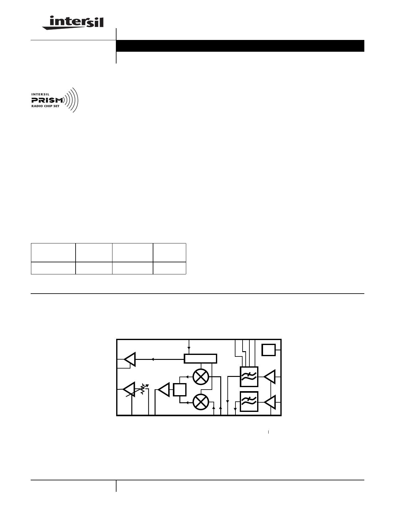
400MHz Quadrature Modulator and AGC
™ The HFA3763 is a highly integrated
baseband converter for quadrature
modulation applications. The HFA3763
400MHz quadrature modulator and
AGC is one of the seven chips in the
PRISM® full duplex chip set (see Typical Application
Diagram). It features all the necessary blocks for baseband
modulation of I and Q signals. An output AGC and Baseband
shaping filters are integrated in the design. Four filter
bandwidths are programmable via a two bit digital control
interface. In addition, these filters are continuously tunable
over a ±20% frequency range via one external resistor. The
modulator channel receives digital or analog I and Q data for
processing. To achieve broadband operation, the Local
Oscillator frequency input is required to be twice the desired
frequency of modulation. A selectable buffered divide by 2
LO output and a stable reference voltage are provided for
convenience of the user.
Ordering Information
TEMP.
PART NUMBER RANGE (oC)
PACKAGE
PKG. NO.
HFA3763IN
-40 to 85 80 Ld TQFP Q80.14x14
Simplified Block Diagram
Features
• Integrates all IF Transmit Functions
• Broad Frequency Range . . . . . . . . . . . 10MHz to 400MHz
• I/Q Amplitude and Phase Balance . . . . . . . . . . . 0.2dB, 2o
• 5th Order Programmable
Low Pass Filter. . . . . . . . . . . . . . . . . . . 2.2MHz - 17.6MHz
• 400MHz Output AGC Amplifier/Attenuator . . . . . . . .45dB
• Selectable Digital or Analog TX Baseband Inputs
• Low LO Drive Level . . . . . . . . . . . . . . . . . . . . . . . -15dBm
• Fast Transmit-on Switching . . . . . . . . . . . . . . . . . . . . . 1µs
• Power Management/Standby Mode
• Single Supply 2.7V to 5.5V Operation
Applications
• Wireless Local Loop Systems
• Wireless Local Area Networks
• PCMCIA Wireless Duplex Transceivers
• ISM Systems
• TDMA Packet Protocol Radios
• PCS/Wireless PBX
MOD_LO_OUT
LO_GND
IF_OUT
÷2 0o/90o
∑
2V
REF
2V REF
LPF_TXI_IN
I
LPF_TXQ_IN
Q
4-1 CAUTION: These devices are sensitive to electrostatic discharge; follow proper IC Handling Procedures.
http://www.intersil.com or 407-727-9207 | Copyright © Intersil Corporation 1999
PRISM® is a registered trademark of Intersil Corporation. PRISM logo is a trademark of Intersil Corporation.
1 page 
HFA3763
Pin Descriptions (Continued)
PIN SYMBOL
DESCRIPTION
41 Mod_TX_PE Digital input control to enable the Modulator section. Enable logic level is High for transmit.
42 Mod_TX_IF_Out Modulator open collector output, single ended. Termination resistor to VCC with a typical value of 250Ω.
44 Mod_LO_In Single ended local oscillator current input. Frequency of input signal must be twice the required modulator carrier
(2XLO)
LO frequency. Input current is optimum at 200µARMS. Input matching networks and filters can be designed for a
wide range of power and impedances at this port. Typical input impedance is 130Ω.This pin requires AC coupling.
NOTE: High second harmonic content input waveforms may degrade I/Q phase accuracy.
45
Mod_VCC
Modulator supply pin. Use high quality decoupling capacitors right at the pin.
46 Mod_LO_Out Divide by 2 buffered output reference from “Mod_LO_in” input. Used for external applications where the
modulating and demodulating carrier reference frequency is required. 50Ω single end driving capability. AC
coupling is required. This output can be disabled by shorting to VCC or floating pin 50.
47
Mod_VCC
Modulator supply pin. Use high quality decoupling capacitors right at the pin.
48
MOD_BYP
This pin must be connected to pin 49 and decoupled to gnd. (Note 1)
49
MOD_BYP
This pin must be connected to pin 48. (Note 1)
50
LO_GND
When grounded, this pin enables the LO buffer (Mod_LO_Out). When open (NC) it disables the LO buffer.
55 IF_AGC_IN AC coupled input to the AGC amplifier.
57
AGC_VCC
AGC supply pin supply pin. Use high quality decoupling capacitors right at the pin.
59 AGC_CTRL AGC control DC control voltage input requires external resistor to set scale factor. 10K for optimum temp. co. May
require decoupling filtering capacitor.
61
63
65
67
See
Pinout
AGC_VCC
AGC_PE
AGC_IF_OUT
AGC_VCC
GND
AGC supply pin supply pin. Use high quality decoupling capacitors right at the pin.
Digital input control for the AGC amplifier. Enable logic level is High.
AGC amplifier output. Output impedance of 250Ω. Need to be connected to VCC by an inductor with reactance
well above 250Ω.
AGC supply pin supply pin. Use high quality decoupling capacitors right at the pin.
All remaining pins not listed above must be connected to a solid ground plane.
NOTE:
1. If pin 50 is grounded, otherwise float.
4-5
5 Page | ||
| Páginas | Total 10 Páginas | |
| PDF Descargar | [ Datasheet HFA3763IN.PDF ] | |
Hoja de datos destacado
| Número de pieza | Descripción | Fabricantes |
| HFA3763IN | 400MHz Quadrature Modulator and AGC | Intersil Corporation |
| Número de pieza | Descripción | Fabricantes |
| SLA6805M | High Voltage 3 phase Motor Driver IC. |
Sanken |
| SDC1742 | 12- and 14-Bit Hybrid Synchro / Resolver-to-Digital Converters. |
Analog Devices |
|
DataSheet.es es una pagina web que funciona como un repositorio de manuales o hoja de datos de muchos de los productos más populares, |
| DataSheet.es | 2020 | Privacy Policy | Contacto | Buscar |