|
|
|
PDF HFA3860IV96 Data sheet ( Hoja de datos )
| Número de pieza | HFA3860IV96 | |
| Descripción | 11 Mbps Direct Sequence Spread Spectrum Baseband Processor | |
| Fabricantes | Intersil Corporation | |
| Logotipo | ||
Hay una vista previa y un enlace de descarga de HFA3860IV96 (archivo pdf) en la parte inferior de esta página. Total 30 Páginas | ||
|
No Preview Available !
Data Sheet
HFA3860
July 1998
File Number 4347
11 Mbps Direct Sequence Spread
Spectrum Baseband Processor
™ The Intersil HFA3860 Direct Sequence
(DSSS) baseband processor is part of
the PRISM 2.4GHz radio chipset, and
contains all the functions necessary for
a full or half duplex packet baseband
transceiver for applications requiring 11 Mbps performance.
The HFA3860 has on-board A/Ds for analog I and Q inputs, for
which the HFA3726 IF QMODEM is recommended. Differential
phase shift keying modulation schemes DBPSK and DQPSK,
with data scrambling capability are available, along with M-Ary
Bi-Orthogonal Keying to provide a variety of data rates. Built-in
flexibility allows the HFA3860 to be configured through a
general purpose control bus, for a range of applications. A
Receive Signal Strength Indicator (RSSI) monitoring function
with on-board 6-bit A/D provides Clear Channel Assessment
(CCA) to avoid data collisions and optimize network throughput.
The HFA3860 is housed in a thin plastic quad flat package
(TQFP) suitable for PCMCIA board applications.
Ordering Information
PART NO.
HFA3860IV
HFA3860IV96
TEMP.
RANGE (oC)
-40 to 85
-40 to 85
PKG. TYPE
48 Ld TQFP
Tape and Reel
PKG. NO.
Q48.7x7
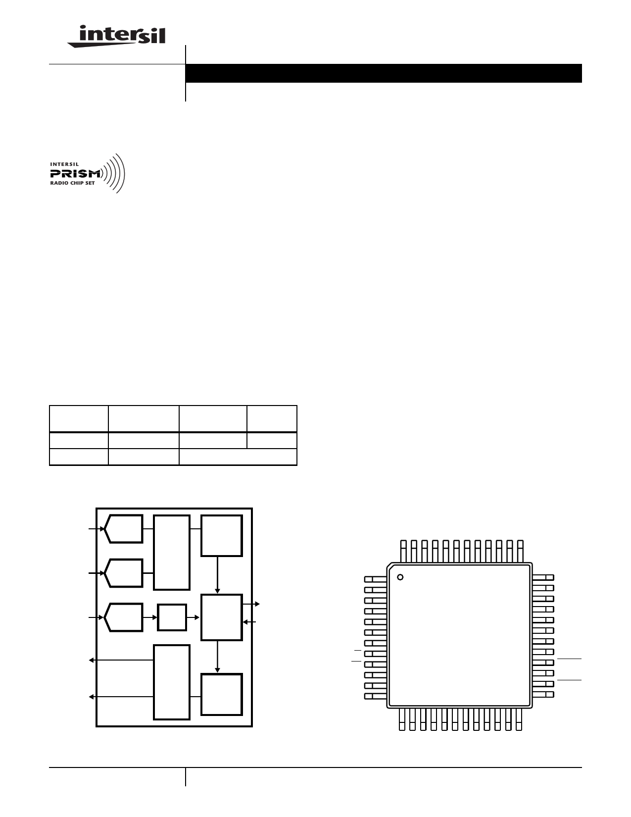
Simplified Block Diagram
IIN
3-BIT
A/D
QIN
3-BIT
A/D
RSSI
6-BIT
A/D
IOUT
DEMOD.
CCA
PRO-
CESSOR
INTER-
FACE
CTRL
QOUT
MOD.
Features
• Complete DSSS Baseband Processor
• Processing Gain . . . . . . . . . . . . . . . . . . . . . . . . . . ≥10.4dB
• Programmable Data Rate. . . . . . . . 1, 2, 5.5, and 11 Mbps
• Ultra Small Package . . . . . . . . . . . . . . . . . . . . 7 x 7 x 1mm
• Single Supply Operation (44MHz Max) . . . . . 2.7V to 3.6V
• Modulation Methods . . . . . . .DBPSK, DQPSK, and MBOK
• Supports Full or Half Duplex Operations
• On-Chip A/D Converters for I/Q Data (3-Bit, 22 MSPS)
and RSSI (6-Bit)
• Similar Pinout to HFA3824
Applications
• Systems Targeting IEEE 802.11 WLAN Standard
• Point-to-Point Links
• DSSS PCMCIA Wireless Transceiver
• Spread Spectrum WLAN RF Modems
• TDMA Packet Protocol Radios
• Part 15 Compliant Radio Links
• Portable Bar Code Scanners/POS Terminal
• Portable PDA/Notebook Computer
• Wireless Digital Audio
• Wireless Digital Video
• PCN/Wireless PBX
Pinout
HFA3860 (TQFP)
EST_CK
TX_PE
TXD
TXCLK
TX_RDY
GND
VDD
R/W
CS
VDDA
GND
IIN
48 47 46 45 44 43 42 41 40 39 38 37
1 36
2 35
3 34
4 33
5 32
6 31
7 30
8 29
9 28
10 27
11 26
12 25
13 14 15 16 17 18 19 20 21 22 23 24
RXCLK
RXD
MD_RD
RX_PE
CCA
GND
MCLK
VDD
RESET
ANTSE
ANTSE
SD
4-1 CAUTION: These devices are sensitive to electrostatic discharge; follow proper IC Handling Procedures.
http://www.intersil.com or 407-727-9207 | Copyright © Intersil Corporation 1999
PRISM® is a registered trademark of Intersil Corporation. PRISM logo is a trademark of Intersil Corporation.
1 page 
HFA3860
Pin Descriptions (Continued)
NAME
PIN TYPE I/O
DESCRIPTION
TEST_CK
1
O This is the clock that is used in conjunction with the data that is being output from the test bus (TEST
0-7).
RESET
28
I Master reset for device. When active TX and RX functions are disabled. If RESET is kept low the
HFA3860 goes into the power standby mode. RESET does not alter any of the configuration register
values nor does it preset any of the registers into default values. Device requires programming upon
power-up. After RESET is de-activated, RX_PE must be activated for at least 2 MCLKs before RX and
TX functions are restored.
MCLK
30
I Master Clock for device. The nominal frequency of this clock is 44MHz. This is used internally to
generate all other internal necessary clocks and is divided by 2 or 4 for the transceiver clocks.
IOUT 48 O TX Spread baseband I digital output data. Data is output at the chip rate.
QOUT
47
O TX Spread baseband Q digital output data. Data is output at the chip rate.
NOTE: Total of 48 pins; ALL pins are used.
External Interfaces
There are three primary digital interface ports for the
HFA3860 that are used for configuration and during normal
operation of the device as shown in Figure 1. These ports
are:
• The Control Port, which is used to configure, write and/or
read the status of the internal HFA3860 registers.
• The TX Port, which is used to accept the data that needs
to be transmitted from the network processor.
• The RX Port, which is used to output the received
demodulated data to the network processor.
In addition to these primary digital interfaces the device
includes a byte wide parallel Test Port which can be
configured to output various internal signals and/or data.
The device can also be set into various power consumption
modes by external control. The HFA3860 contains three
Analog to Digital (A/D) converters. The analog interfaces to
the HFA3860 include, the In phase (I) and quadrature (Q)
data component inputs, and the RF signal strength indicator
input. A reference voltage divider is also required external to
the device.
ANTSEL
HFA3860
ANALOG
INPUTS
A/D
REFERENCE
POWER
DOWN
SIGNALS
TEST
PORT
I (ANALOG)
Q (ANALOG)
TXD
RSSI (ANALOG) TXCLK
TX_RDY
VREFN
VREFP
RXD
RXC
TX_PE
RX_PE
MD_RDY
CS
SD
RESET
SCLK
8
TEST
R/W
SDI
TX_PORT
RX_PORT
CONTROL_PORT
FIGURE 1. EXTERNAL INTERFACE
Control Port (4 Wire)
The serial control port is used to serially write and read data
to/from the device. This serial port can operate up to a
11MHz rate or 1/2 the maximum master clock rate of the
device, MCLK (whichever is lower). MCLK must be running
during programming. This port is used to program and to
read all internal registers. The first 8 bits always represent
the address followed immediately by the 8 data bits for that
register. The two LSBs of address are don’t care, but
reserved for future expansion. The serial transfers are
accomplished through the serial data pin (SD). SD is a
bidirectional serial data bus. Chip Select (CS), and
Read/Write (R/W) are also required as handshake signals
for this port. The clock used in conjunction with the address
and data on SD is SCLK. This clock is provided by the
external source and it is an input to the HFA3860. The timing
relationships of these signals are illustrated in Figures 2 and
3. R/W is high when data is to be read, and low when it is to
be written. CS is an asynchronous reset to the state
machine. CS must be active (low) during the entire data
transfer cycle. CS selects the serial control port device only.
The serial control port operates asynchronously from the TX
and RX ports and it can accomplish data transfers
independent of the activity at the other digital or analog
ports.
The HFA3860 has 32 internal registers that can be accessed
through the control port. These registers are listed in the
Configuration and Control Internal Register table. Table 1 lists
the configuration register number, a brief name describing the
register, and the HEX address to access each of the registers.
The type indicates whether the corresponding register is
Read only (R) or Read/Write (R/W). Some registers are two
bytes wide as indicated on the table (high and low bytes).
See Tech Brief #360 on timing issues between the serial
clock (SCLK) and the chip master clock (MCLK).
4-5
5 Page 
HFA3860
TABLE 5. TEST MODES (Continued)
MODE DESCRIPTION TEST_CLK
TEST (7:0)
10 Bit Sync Accum Sample CLK Bit Sync Accum (7:0)
(0Ah) Lo Rate
11 Reserved
Reserved Factory Test Only
12 A/D Cal Test
Mode
A/D Cal CLK A/DCal, ED, A/DCal
Disable, ADCal (4:0)
13 Correlator I High Sample CLK Correlator I (8:1)
Rate
14 Correlator Q High Sample CLK Correlator Q (8:1)
Rate
15 Chip Error
Accumulator
0
Chip Error Accum
(14:7)
16 NCO Test Hi
Rate
Sample CLK NCO Accum (19:12)
17 Freq Test Hi Rate Sample CLK Lag Accum (18:11)
18 Carrier Phase
Error Hi Rate
Sample CLK Carrier Phase Error
(6,6:0)
19 Reserved
Sample CLK Factory Test Only
20 Reserved
Sample CLK Factory Test Only
21 I_A/D, Q_A/D
Sample CLK 0,0,I_A/D (2:0),Q_A/D
(2:0)
22 Reserved
Reserved Factory Test Only
23 Reserved
Reserved Factory Test Only
24 Reserved
Reserved Factory Test Only
25 A/D Cal Accum A/D Cal
Lo Accum (8)
A/D Cal Accum (7:0)
26 A/D Cal Accum A/D Cal
A/D Cal Accum (16:9)
Hi Accum (17)
27 Freq Accum Lo Freq Accum Freq Accum (14:7)
(15)
28 Reserved
Reserved Factory Test Only
29 SQ2 Monitor Hi Pulse After SQ2 (15:8)
SQ Valid
30-31 Reserved
Reserved Factory Test Only
MODE
SLEEP
RX_PE
Inactive
TX_PE
Inactive
STANDBY Inactive Inactive
TX
Inactive
Active
RX
Active
Inactive
NO CLOCK
ICC Standby
TABLE 6. POWER DOWN MODES
RESET AT 44MHz
DEVICE STATE
Active
4mA
Both transmit and receive functions disabled. Device in sleep mode. Control
Interface is still active. Register values are maintained. Device will return to its
active state within 10µs plus settling time of AC coupling capacitors (about
5ms).
Inactive
11mA
Both transmit and receive operations disabled. Device will resume its
operational state within 1µs of RX_PE or TX_PE going active.
Inactive
15mA
Receiver operations disabled. Receiver will return in its operational state
within 1µs of RX_PE going active.
Inactive
24mA Transmitter operations disabled. Transmitter will return to its operational state
within 2 MCLKs of TX_PE going active.
Active
300µA All inputs at VCC or GND.
4-11
11 Page | ||
| Páginas | Total 30 Páginas | |
| PDF Descargar | [ Datasheet HFA3860IV96.PDF ] | |
Hoja de datos destacado
| Número de pieza | Descripción | Fabricantes |
| HFA3860IV96 | 11 Mbps Direct Sequence Spread Spectrum Baseband Processor | Intersil Corporation |
| Número de pieza | Descripción | Fabricantes |
| SLA6805M | High Voltage 3 phase Motor Driver IC. |
Sanken |
| SDC1742 | 12- and 14-Bit Hybrid Synchro / Resolver-to-Digital Converters. |
Analog Devices |
|
DataSheet.es es una pagina web que funciona como un repositorio de manuales o hoja de datos de muchos de los productos más populares, |
| DataSheet.es | 2020 | Privacy Policy | Contacto | Buscar |