|
|
|
PDF NCV331 Data sheet ( Hoja de datos )
| Número de pieza | NCV331 | |
| Descripción | Low Voltage Comparators | |
| Fabricantes | ON Semiconductor | |
| Logotipo | ||
Hay una vista previa y un enlace de descarga de NCV331 (archivo pdf) en la parte inferior de esta página. Total 19 Páginas | ||
|
No Preview Available !
LMV331, NCV331, LMV393,
LMV339
Single, Dual, Quad General
Purpose, Low Voltage
Comparators
The LMV331 is a CMOS single channel, general purpose, low
voltage comparator. The LMV393 and LMV339 are dual and quad
channel versions, respectively. The LMV331/393/339 are specified
for 2.7 V to 5 V performance, have excellent input common−mode
range, low quiescent current, and are available in several space saving
packages.
The LMV331 is available in 5−pin SC−70 and TSOP−5 packages.
The LMV393 is available in a 8−pin Micro8t, SOIC−8, and a
UDFN8 package, and the LMV339 is available in a SOIC−14 and a
TSSOP−14 package.
The LMV331/393/339 are cost effective solutions for applications
where space saving, low voltage operation, and low power are the
primary specifications in circuit design for portable applications.
Features
• Guaranteed 2.7 V and 5 V Performance
• Input Common−mode Voltage Range Extends to Ground
• Open Drain Output for Wired−OR Applications
• Low Quiescent Current: 60 mA/channel TYP @ 5 V
• Low Saturation Voltage 200 mV TYP @ 5 V
• Propagation Delay 200 ns TYP @ 5 V
• NCV Prefix for Automotive and Other Applications Requiring
Unique Site and Control Change Requirements; AEC−Q100
Qualified and PPAP Capable
• These Devices are Pb−Free, Halogen Free/BFR Free and are RoHS
Compliant
Typical Applications
• Battery Monitors
• Notebooks and PDA’s
• General Purpose Portable Devices
• General Purpose Low Voltage Applications
+VCC
http://onsemi.com
1
SC−70
CASE 419A
5
1
TSOP−5
CASE 483
1
Micro8
CASE 846A
8
1
SOIC−8
CASE 751
8
1
UDFN8
CASE 517AJ
1
SOIC−14
CASE 751A
1
TSSOP−14
CASE 948G
ORDERING INFORMATION
See detailed ordering and shipping information in the package
dimensions section on page 13 of this data sheet.
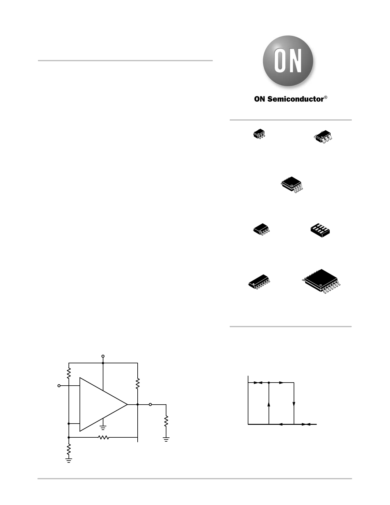
R1
VIN
V+
R2
− RPULL−UP
VO
+ RLOAD
R3
Figure 1. Inverting
Comparator with Hysteresis
VCC
VO
0
VT2
VIN
VT1
Figure 2. Hysteresis Curve
© Semiconductor Components Industries, LLC, 2014
November, 2014 − Rev. 7
1
Publication Order Number:
LMV331/D
1 page 
LMV331, NCV331, LMV393, LMV339
5.0 V DC ELECTRICAL CHARACTERISTICS (All limits are guaranteed for TA = 25°C, V+ = 5 V, V− = 0 V, VCM = 2.5 V unless
otherwise noted.)
Parameter
Symbol
Condition (Note 6)
Min
Typ Max Unit
Input Offset Voltage
Input Offset Voltage Average Drift
Input Bias Current (Note 5)
Input Offset Current (Note 5)
Input Voltage Range
Voltage Gain (Note 5)
Saturation Voltage
VIO
IB
IIO
VCM
AV
VSAT
TA = TLO to THIGH
TA = TLO to THIGH
TA = TLO to THIGH
TA = TLO to THIGH
TA = TLO to THIGH
1.7 9 mV
5 mV/°C
< 1 nA
< 1 nA
0 to 4.2
V
20 50
V/mV
200 400 mV
700
Output Sink Current
IO VO ≤ 1.5 V 10 84
mA
Supply Current
LMV331
ICC
TA = TLO to THIGH
60 120 mA
150
Supply Current
LMV393
ICC
TA = TLO to THIGH
100 200 mA
250
Supply Current
LMV339
ICC
TA = TLO to THIGH
170 300 mA
350
Output Leakage Current (Note 5)
TA = TLO to THIGH
0.003
1
5.0 V AC ELECTRICAL CHARACTERISTICS (TA = 25°C, V+ = 5 V, RL = 5.1 kW, V− = 0 V unless otherwise noted.)
Parameter
Symbol
Condition
Min Typ Max
mA
Unit
Propagation Delay − High to Low
tPHL Input Overdrive = 10 mV
Input Overdrive = 100 mV
1500
900
ns
Propagation Delay − Low to High
tPLH Input Overdrive = 10 mV
Input Overdrive = 100 mV
800
200
ns
5. Guaranteed by design and/or characterization.
6. For LMV331, LMV393, LMV339: TA = −40°C to 85°C
For NCV331: TA = −40°C to 125°C
http://onsemi.com
5
5 Page 
LMV331, NCV331, LMV393, LMV339
APPLICATION CIRCUITS
Basic Comparator Operation
The basic operation of a comparator is to compare two
input voltage signals, and produce a digital output signal by
determining which input signal is higher. If the voltage on
the non−inverting input is higher, then the internal output
transistor is off and the output will be high. If the voltage on
the inverting input is higher, then the output transistor will
be on and the output will be low. The LMV331/393/339 has
an open−drain output stage, so a pull−up resistor to a positive
supply voltage is required for the output to switch properly.
The size of the pull−up resistor is recommended to be
between 1 kW and 10 kW. This range of values will balance
two key factors; i.e., power dissipation and drive capability
for interface circuitry.
Figure 19 illustrates the basic operation of a comparator
and assumes dual supplies. The comparator compares the
input voltage (VIN) on the non−inverting input to the
reference voltage (VREF) on the inverting input. If VIN is less
than VREF, the output voltage (VO) will be low. If VIN is
greater than VREF, then VO will be high.
R1
VIN
V+
R2
+VCC
−
+
R3
RPULL−UP
VO
RLOAD
Figure 20. Inverting
Comparator with
Hysteresis
VOUT
V+
VREF
0V
VIN
+VIN
+
Time
V+
3.0 k
VO
+VREF
−
Figure 19.
Comparators and Stability
A common problem with comparators is oscillation due to
their high gain. The basic comparator configuration in
Figure 19 may oscillate if the differential voltage between
the input pins is close to the device’s offset voltage. This can
happen if the input signal is moving slowly through the
comparator’s switching threshold or if unused channels are
connected to the same potential for termination of unused
channels. One way to eliminate output oscillations or
‘chatter’ is to include external hysteresis in the circuit
design.
Inverting Configuration with Hysteresis
An inverting comparator with hysteresis is shown in
Figure 20.
When VIN is less than the voltage at the non−inverting
node, V+, the output voltage will be high. When VIN is
greater than the voltage at V+, then the output will be low.
The hysteresis band (Figure 21) created from the resistor
network is defined as:
DV) + VT1 * VT2
where VT1 and VT2 are the lower and upper trip points,
respectively.
VCC
VO
0
VT2
VIN
VT1
Figure 21.
VT1 is calculated by assuming that the output of the
comparator is pulled up to supply when high. The
resistances R1 and R3 can be viewed as being in parallel
which is in series with R2 (Figure 22). Therefore VT1 is:
VT1
+
ǒR1
VCC R2
ø R3Ǔ )
R2
VT2 is calculated by assuming that the output of the
comparator is at ground potential when low. The resistances
R2 and R3 can be viewed as being in parallel which is in
series with R1 (Figure 23). Therefore VT2 is:
VT2
+
VCCǒR2 ø R3Ǔ
R1 ) ǒR2 ø R3Ǔ
http://onsemi.com
11
11 Page | ||
| Páginas | Total 19 Páginas | |
| PDF Descargar | [ Datasheet NCV331.PDF ] | |
Hoja de datos destacado
| Número de pieza | Descripción | Fabricantes |
| NCV33033 | Brushless DC Motor Controller | ON Semiconductor |
| NCV33035 | Brushless DC Motor Controller | ON |
| NCV33035DWR2 | Brushless DC Motor Controller | ON |
| NCV33039 | Closed Loop Brushless Motor Adapter | ON Semiconductor |
| Número de pieza | Descripción | Fabricantes |
| SLA6805M | High Voltage 3 phase Motor Driver IC. |
Sanken |
| SDC1742 | 12- and 14-Bit Hybrid Synchro / Resolver-to-Digital Converters. |
Analog Devices |
|
DataSheet.es es una pagina web que funciona como un repositorio de manuales o hoja de datos de muchos de los productos más populares, |
| DataSheet.es | 2020 | Privacy Policy | Contacto | Buscar |