|
|
|
PDF NCS36000 Data sheet ( Hoja de datos )
| Número de pieza | NCS36000 | |
| Descripción | Passive Infrared (PIR) Detector Controller | |
| Fabricantes | ON Semiconductor | |
| Logotipo | ||
Hay una vista previa y un enlace de descarga de NCS36000 (archivo pdf) en la parte inferior de esta página. Total 8 Páginas | ||
|
No Preview Available !
NCS36000
Passive Infrared (PIR)
Detector Controller
The NCS36000 is a fully integrated mixed−signal CMOS device
designed for low−cost passive infrared controlling applications. The
device integrates two low−noise amplifiers and a LDO regulator to
drive the sensor. The output of the amplifiers goes to a window
comparator that uses internal voltage references from the regulator.
The digital control circuit processes the output from the window
comparator and provides the output to the OUT and LED pin.
Features
• 3.0 − 5.75 V Operation
• −40 to 85°C
• 14 Pin SOIC Package
• Integrated 2−Stage Amplifier
• Internal LDO to Drive Sensor
• Internal Oscillator with External RC
• Single or Dual Pulse Detection
• Direct Drive of LED and OUT
• This is a Pb−Free Device
Typical Applications
• Automatic Lighting (Residential and Commercial)
• Automation of Doors
• Motion Triggered Events (Animal photography)
www.onsemi.com
MARKING
DIAGRAM
14
1
SOIC−14
D SUFFIX
CASE 751A
14
NCS36000G
AWLYWW
1
A = Assembly Location
WL = Wafer Lot
Y = Year
WW = Work Week
G = Pb−Free Package
PIN CONNECTIONS
OP2_O 1
OP2_N 2
OP1_O 3
OP1_N 4
OP1_P 5
VREF 6
VSS 7
14 VDD
13 OSC
12 MODE
11 NC
10 xLED_EN
9 LED
8 OUT
(Top View)
VREF 6
OP1_P 5
OP1_N 4
OP1_O 3
OP2_N 2
OP2_O 1
OSC 13
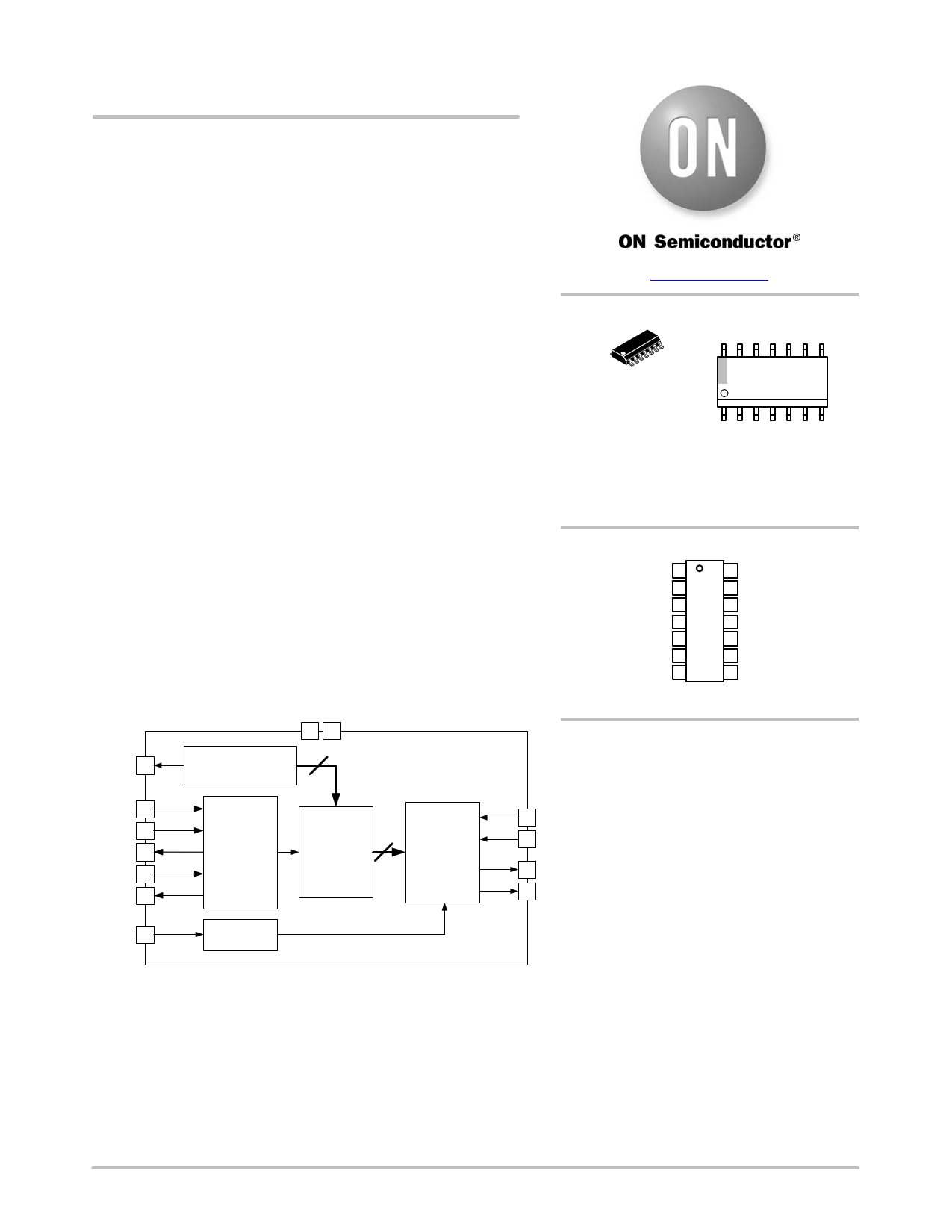
LDO &
Voltage References
2
Amplifier
Circuit
Window 2
Comparator
System
Oscillator
Digital
Control
Circuit
ORDERING INFORMATION
See detailed ordering and shipping information in the package
dimensions section on page 7 of this data sheet.
12 MODE
10 xLED_EN
9 LED
8 OUT
Figure 1. Simplified Block Diagram
© Semiconductor Components Industries, LLC, 2015
December, 2015 − Rev. 3
1
Publication Order Number:
NCS36000/D
1 page 
NCS36000
VREF 6
LDO
D Vm +
5+
G 3 2−
4−
Sensor dependent
components
Application dependent
components
Vh
OP2_O
1
Vl
−
Comp_P
+
−
Comp_N
+
VREF 6
Vh
Vm
Vl
Figure 5. Figure Showing Simplified Block Diagram of Analog Conditioning Stages
Digital Signal Processing Block (all times assume a
62.5 Hz system oscillator frequency)
The digital signaling processing block performs three
major functions.
The first function is that the device toggles LED during the
start−up sequencing at approximately two hertz regardless
of the state of the XLED_EN pin. The startup sequence lasts
for thirty seconds. During that time the OUT pin is held low
regardless of the state of OP2_O.
The second function of the digital signal processing block
is to insure a certain glitch width is seen before OUT is
toggled. The digital signal processing block is synchronous
with the system oscillator frequency and therefore the
deglitch time is related to when the comparators toggle
within the oscillator period. A signal width less than two
clock period is guaranteed to be deglitched as a zero. A
signal width of greater than three clock cycles is guaranteed
to be de−glitched. It should be noted that down−sampling
can occur if sufficient anti−aliasing is not performed at the
input of the circuit (OPI_P) or if noise is injected into the
amplifiers, an example would be a noisy power supply.
The third function of the digital signal processing block is
to recognize different pulse signatures coming from the
window comparator block. The device is equipped with two
pulse recognition routines. Single pulse mode (MODE tied
to VSS) will trigger the OUT pin if either comparator toggles
and the deglitch time is of the appropriate length. (See
Figure 6). Dual pulse mode (MODE tied to VDD) requires
two pulses with each pulse coming from the opposite
comparator to occur within a timeout window of five
seconds or 312 clock cycles (See Figure 7). If the adjacent
pulses occur outside the timeout window then the digital
processing block will restart the pulse recognition routine.
xLED_EN Pin
The xLED_EN pin enables the LED output driver when
motion has been detected. If xLED_EN is tied high the LED
pin will not toggle after motion is detected. If the xLED_EN
is tied low the LED pin will toggle when motion is detected.
During start-up the LED pin will toggle irrespective of how
the xLED_EN pin is tied. (See Figure 6).
OP 2_O
VH = 2,5V
VM = 2,1V
VL = 1,7V
TSP< 3TCLK
TSP > 3TCLK
4TCLK
OUT
120 TCLK
Figure 6. Timing Diagram for Single−Pulse Mode Detection
www.onsemi.com
5
5 Page | ||
| Páginas | Total 8 Páginas | |
| PDF Descargar | [ Datasheet NCS36000.PDF ] | |
Hoja de datos destacado
| Número de pieza | Descripción | Fabricantes |
| NCS36000 | Passive Infrared (PIR) Detector Controller | ON Semiconductor |
| Número de pieza | Descripción | Fabricantes |
| SLA6805M | High Voltage 3 phase Motor Driver IC. |
Sanken |
| SDC1742 | 12- and 14-Bit Hybrid Synchro / Resolver-to-Digital Converters. |
Analog Devices |
|
DataSheet.es es una pagina web que funciona como un repositorio de manuales o hoja de datos de muchos de los productos más populares, |
| DataSheet.es | 2020 | Privacy Policy | Contacto | Buscar |