|
|
|
PDF NCP5228 Data sheet ( Hoja de datos )
| Número de pieza | NCP5228 | |
| Descripción | Synchronous Buck Controller | |
| Fabricantes | ON Semiconductor | |
| Logotipo | ||
Hay una vista previa y un enlace de descarga de NCP5228 (archivo pdf) en la parte inferior de esta página. Total 11 Páginas | ||
|
No Preview Available !
NCP5228
Advance Information
Synchronous Buck Controller
with Auto Power Saving
Mode and Built-In LDO
NCP5228 is a dual synchronous buck controller that is optimized for
converting the battery voltage or adaptor voltage into multiple power
rails required in desktop and notebook system. NCP5228 consists of
two buck switching controllers with fixed 5.0 V output on channel 2,
3.3 V on channel 1 and two on−board LDOs with three outputs: 5 V /
60 mA and 3.3 V or 12 V / 10 mA. NCP5228 supports high efficiency,
fast transient response and provides power good signals. ON
Semiconductor proprietary adaptive−ripple control enables seamless
transition from CCM to DCM, where converter runs at reduced
switching frequency with much higher efficiency at light load. The
part operates with supply voltage ranging from 5.5 V to 28 V.
NCP5228 is available in a 28−pin QFN package.
Features
• Wide Input Voltage Range: from 5.5 V to 28 V
• Built−in 5 V / 60 mA LDO
• Built−in selectable 3.3 V or 12 V / 10 mA LDO
• Three Selectable Fixed Frequency 300 KHz, 400 KHz or 600 KHz
• 180 Interleaved Operation Between the Two Channels in
Continue−Conduction−Mode (CCM)
• Selected Power−Saving Mode/Forced PWM Mode
• Transient−Response−Enhancement (TRE) Control
• Input Supply Voltage Feed Forward Control
• Resistive or Lossless Inductor’s DCR Current Sensing
• Over−Temperature Protection
• Internal Fixed 13 ms Soft−Start
• Fixed Output Voltages 5 V and 3.3 V
• Power Good Outputs for Both Channels
• Built−in Adaptive Gate Drivers
• Output Discharge Operation
• Built−in Over−Voltage, Under−Voltage Protection
• Accurate Over−Current Protection
• Thermal Shutdown
• This is a Pb−Free Device
Applications
• Desktop / Notebook Computers
• System Power Supplies
• I/O Power Supplies
This document contains information on a new product. Specifications and information
herein are subject to change without notice.
http://onsemi.com
1
28 PIN QFN, 4x4
MN SUFFIX
CASE 485AR
MARKING
DIAGRAM
NCP5228
ALYWG
G
NCP5228 = Specific Device Code
A = Assembly Location
L = Wafer Lot
Y = Year
W = Work Week
G = Pb−Free Package
(Note: Microdot may be in either location)
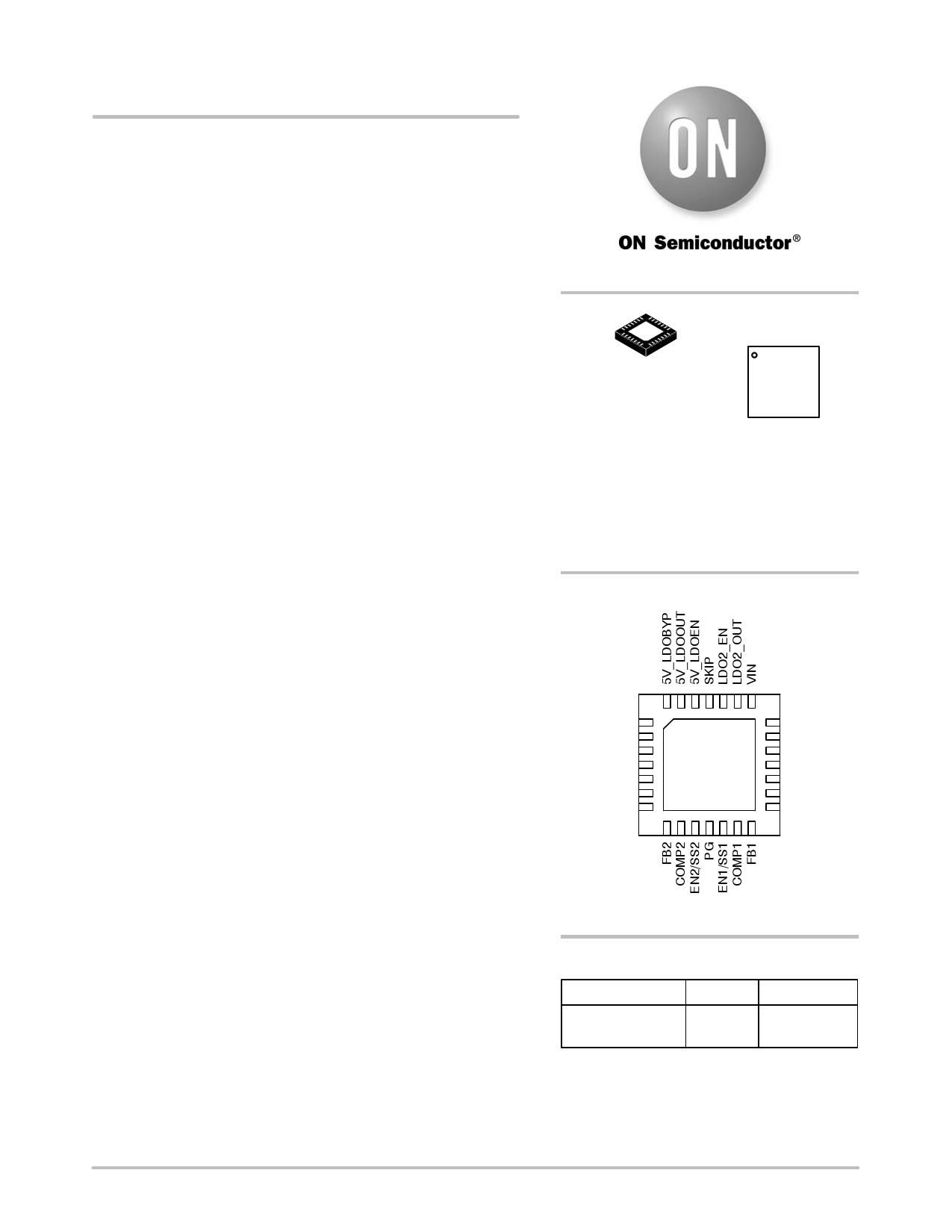
PIN CONNECTIONS
GH2
BST2
SWN2
GL2
PGND2
CSP2
CSN2
28
1
GND
GH1
BST1
SWN1
GL1/FSET
PGND1
CSP1
CSN1
(Top View)
ORDERING INFORMATION
Device
Package
Shipping†
NCP5228MNTWG
QFN−28
(Pb−Free)
4,000 /
Tape & Reel
†For information on tape and reel specifications,
including part orientation and tape sizes, please
refer to our Tape and Reel Packaging Specification
Brochure, BRD8011/D.
© Semiconductor Components Industries, LLC, 2013
October, 2013 − Rev. P6
1
Publication Order Number:
NCP5228/D
1 page 
NCP5228
Table 3. ELECTRICAL CHARACTERISTICS
(VIN = 12 V, Vout = 5.0 V, TA = +25°C for typical value; 0°C < TA < 85°C for min/max values unless noted otherwise)
Parameter
Symbol
Test Conditions
Min Typ Max Units
POWER SUPPLY
Input supply voltage
VIN
5.5 28 V
INTERNAL LDO OUTPUT
5V_LDOOUT Voltage
5V_LDOOUT Current
VIN =12 V, I5V_LDOOUT = 60 mA
VIN =12 V, EN1 = EN2 = 0
4.9 5.0 5.15
V
100 mA
5V_LDO Switch to Bypass Threshold
4.75 4.95 V
5V_LDOOUT to 5V_LDOBYP Impedance
Hysteresis
LDOBYP = 5 V
1.0
100 200
W
mV
LDO2_OUT Voltage
LDO2_EN = VCC, VIN = 15 V,
Load Current = 10 mA
11.4 12.0 12.6
V
LDO2_EN = 1/2 VCC, VIN = 15 V,
Load Current = 10 mA
3.20 3.33 3.46
V
LDO2_OUT Current
10 15
mA
SUPPLY CURRENT
BSTx Quiescent Current
IBST VFB = 1.5 V, EN = 5.0
(No Switching), GH and GL are open
0.3 mA
BSTx Shutdown Supply Current
Vin Pin Supply Current
IBST_SD
EN = 0, BST = 5 V, SWN = 0
Iload = 0
6.0
2.0
mA
mA
Shutdown Current
IVIN_SD
EN1, EN2, LDOEN, LDO2_EN = 0
EN1, EN2, LDOEN = 5 V,
LDO2_EN = 5 V
5.0 mA
1.15 mA
EN1, EN2 = 0, LDOEN = 5 V,
LDO2_EN = 2.5 V
1.57 mA
EN1, EN2 = 0, LDOEN = 5 V,
LDO2_EN = 0
1.11 mA
OSCILLATOR
Oscillator Frequency
Fsw Rset = 1.8 k
270 300 330
KHz
Rset = 9.1 k
340 400 460
KHz
Rset = 16 k
540 600 660
KHz
Oscillator Frequency Accuracy
ERROR AMPLIFIER
±10 %
Open Loop DC Gain (Note 3)
80 dB
Open Loop Unity Gain Bandwidth (Note 3)
Open Loop Phase Margin (Note 3)
F0dB,EA
10 15
60
MHz
deg
Input Bias Current (Note 3)
−200
200 nA
Input Offset Voltage (Note 3)
V+ = V− = 0.8 V
−1.0 1.0 mV
Slew Rate
Maximum Output Voltage
Minimum Output Voltage
Output Source Current
Output Sink Current
3. Guaranteed by Design
4. Parameters are for design only, not for product test.
COMP pin to GND = 10 pF
2.5
10 mV of overdrive, ISOURCE = 2.0 mA
10 mV of overdrive, ISINK = 2.0 mA
10 mV of overdrive, Vout = 3.5 V
10 mV of overdrive, Vout = 1.0 V
3.3
2.0
2.0
0.3
V/ms
V
V
mA
mA
http://onsemi.com
5
5 Page 
NCP5228
PACKAGE DIMENSIONS
ÇÇÇÇPIN ONE
ÇÇÇÇÇÇÇÇÇÇÇÇREFERENCE
D
0.10 C
0.10 C
0.10 C
TOP VIEW
DETAIL B
QFN28 4x4, 0.4P
CASE 485AR
ISSUE A
AB
LL
L1
E
A
A3
DETAIL A
ALTERNATE TERMINAL
CONSTRUCTIONS
ÉÉÉÉEXPOSED Cu
MOLD CMPD
DETAIL B
ALTERNATE
CONSTRUCTION
NOTES:
1. DIMENSIONING AND TOLERANCING PER ASME
Y14.5M, 1994.
2. CONTROLLING DIMENSION: MILLIMETERS.
3. DIMENSION b APPLIES TO PLATED TERMINAL
AND IS MEASURED BETWEEN 0.15 AND 0.30 MM
FROM THE TERMINAL TIP.
4. COPLANARITY APPLIES TO THE EXPOSED PAD
AS WELL AS THE TERMINALS.
MILLIMETERS
DIM MIN MAX
A 0.80 1.00
A1 0.00 0.05
A3 0.20 REF
b 0.15 0.25
D 4.00 BSC
D2 2.50 2.70
E 4.00 BSC
E2 2.50 2.70
e 0.40 BSC
K 0.30 REF
L 0.30 0.50
L1 −−− 0.15
0.08 C
NOTE 4
SIDE VIEW
DETAIL A
8
28X L
D2
A1
C
SEATING
PLANE
0.10 C A B
K
15 0.10 C A B
E2
PIN 1
INDICATOR
1
e 22
BOTTOM VIEW
28X b
0.07
0.05
CAB
C NOTE 3
RECOMMENDED
MOUNTING FOOTPRINT
4.30
2.71
28X
0.62
1
2.71 4.30
PACKAGE
OUTLINE
0.40
PITCH
28X
0.26
DIMENSIONS: MILLIMETERS
ON Semiconductor and
are registered trademarks of Semiconductor Components Industries, LLC (SCILLC). SCILLC owns the rights to a number of patents, trademarks,
copyrights, trade secrets, and other intellectual property. A listing of SCILLC’s product/patent coverage may be accessed at www.onsemi.com/site/pdf/Patent−Marking.pdf. SCILLC
reserves the right to make changes without further notice to any products herein. SCILLC makes no warranty, representation or guarantee regarding the suitability of its products for any
particular purpose, nor does SCILLC assume any liability arising out of the application or use of any product or circuit, and specifically disclaims any and all liability, including without
limitation special, consequential or incidental damages. “Typical” parameters which may be provided in SCILLC data sheets and/or specifications can and do vary in different applications
and actual performance may vary over time. All operating parameters, including “Typicals” must be validated for each customer application by customer’s technical experts. SCILLC
does not convey any license under its patent rights nor the rights of others. SCILLC products are not designed, intended, or authorized for use as components in systems intended for
surgical implant into the body, or other applications intended to support or sustain life, or for any other application in which the failure of the SCILLC product could create a situation where
personal injury or death may occur. Should Buyer purchase or use SCILLC products for any such unintended or unauthorized application, Buyer shall indemnify and hold SCILLC and
its officers, employees, subsidiaries, affiliates, and distributors harmless against all claims, costs, damages, and expenses, and reasonable attorney fees arising out of, directly or indirectly,
any claim of personal injury or death associated with such unintended or unauthorized use, even if such claim alleges that SCILLC was negligent regarding the design or manufacture
of the part. SCILLC is an Equal Opportunity/Affirmative Action Employer. This literature is subject to all applicable copyright laws and is not for resale in any manner.
PUBLICATION ORDERING INFORMATION
LITERATURE FULFILLMENT:
Literature Distribution Center for ON Semiconductor
P.O. Box 5163, Denver, Colorado 80217 USA
Phone: 303−675−2175 or 800−344−3860 Toll Free USA/Canada
Fax: 303−675−2176 or 800−344−3867 Toll Free USA/Canada
Email: [email protected]
N. American Technical Support: 800−282−9855 Toll Free
USA/Canada
Europe, Middle East and Africa Technical Support:
Phone: 421 33 790 2910
Japan Customer Focus Center
Phone: 81−3−5817−1050
http://onsemi.com
11
ON Semiconductor Website: www.onsemi.com
Order Literature: http://www.onsemi.com/orderlit
For additional information, please contact your local
Sales Representative
NCP5228/D
11 Page | ||
| Páginas | Total 11 Páginas | |
| PDF Descargar | [ Datasheet NCP5228.PDF ] | |
Hoja de datos destacado
| Número de pieza | Descripción | Fabricantes |
| NCP5220 | PWM Dual Buck and Linear Power Controller | ON Semiconductor |
| NCP5220A | 3-in-1 PWM Dual Buck and Linear Power Controller | ON Semiconductor |
| NCP5222 | High Performance Dual-Channel / Two-Phase Synchronous Buck Controller | ON Semiconductor |
| NCP5228 | Synchronous Buck Controller | ON Semiconductor |
| Número de pieza | Descripción | Fabricantes |
| SLA6805M | High Voltage 3 phase Motor Driver IC. |
Sanken |
| SDC1742 | 12- and 14-Bit Hybrid Synchro / Resolver-to-Digital Converters. |
Analog Devices |
|
DataSheet.es es una pagina web que funciona como un repositorio de manuales o hoja de datos de muchos de los productos más populares, |
| DataSheet.es | 2020 | Privacy Policy | Contacto | Buscar |