|
|
|
PDF HC123 Data sheet ( Hoja de datos )
| Número de pieza | HC123 | |
| Descripción | Dual Retriggerable Monostable Multivibrator | |
| Fabricantes | Fairchild Semiconductor | |
| Logotipo | ||
Hay una vista previa y un enlace de descarga de HC123 (archivo pdf) en la parte inferior de esta página. Total 9 Páginas | ||
|
No Preview Available !
July 1993
Revised April 1999
74VHC123A
Dual Retriggerable Monostable Multivibrator
General Description
The VHC123A is an advanced high speed CMOS
Monostable Multivibrator fabricated with silicon gate CMOS
technology. It achieves the high speed operation similar to
equivalent Bipolar Schottky TTL while maintaining the
CMOS low power dissipation. Each multivibrator features
both a negative, A, and a positive, B, transition triggered
input, either of which can be used as an inhibit input. Also
included is a clear input that when taken low resets the
one-shot. The VHC123A can be triggered on the positive
transition of the clear while A is held low and B is held high.
The output pulse width is determined by the equation:
PW = (Rx)(Cx); where PW is in seconds, R is in ohms, and
C is in farads.
Limits for Rx and Cx are:
External capacitor, Cx No limit
External resistors, Rx VCC = 2.0V, 5 kΩ min
VCC > 3.0V, 1 kΩ min
An input protection circuit ensures that 0 to 7V can be
applied to the input pins without regard to the supply volt-
age. This device can be used to interface 5V to 3V systems
and two supply systems such as battery back up. This cir-
cuit prevents device destruction due to mismatched supply
and input voltages.
Features
s High Speed:
tPD = 8.1 ns (typ) at TA = 25°C
s Low Power Dissipation:
ICC = 4 µA (Max) at TA = 25°C
s Active State: ICC = 600 µA (Max) at TA = 25°C
s High Noise Immunity: VNIH = VNIL = 28% VCC (min)
s Power down protection is provided on all inputs
s Pin and function compatible with 74HC123A
Ordering Code:
Order Number Package Number
Package Description
74VHC123AM
M16A
16-Lead Small Outline Integrated Circuit (SOIC), JEDEC MS-012, 0.150” Narrow
74VHC123ASJ
M16D
16-Lead Small Outline Package (SOP), EIAJ TYPE II, 5.3mm Wide
74VHC123AMTC
MTC16
16-Lead Thin Shrink Small Outline Package (TSSOP), JEDEC MO-153, 4.4mm Wide
74VHC123AN
N16E
16-Lead Plastic Dual-In-Line Package (PDIP), JEDEC MS-001, 0.300” Wide
Surface mount packages are also available on Tape and Reel. Specify by appending the suffix letter “X” to the ordering code.
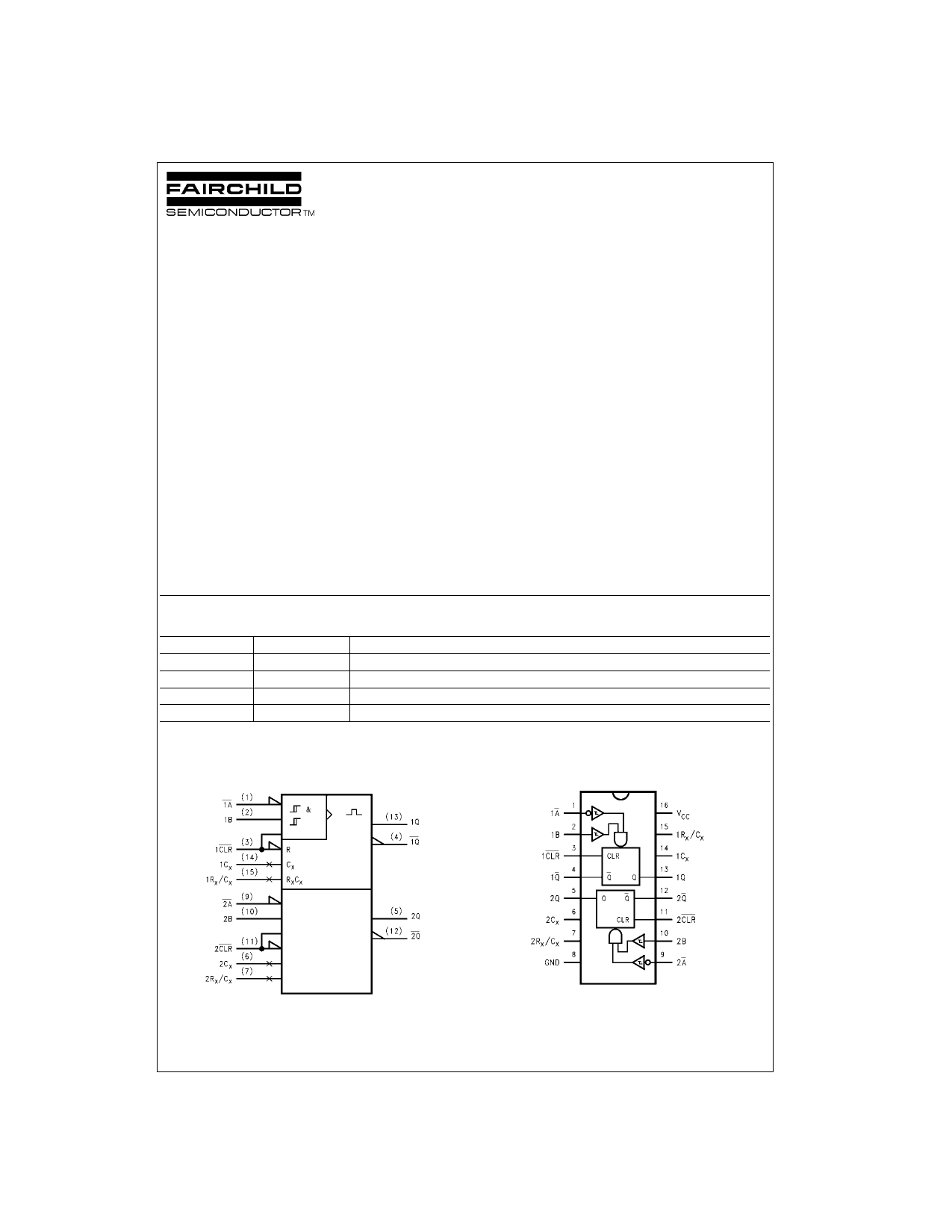
Logic Symbol
Connection Diagram
IEEE/IEC
© 1999 Fairchild Semiconductor Corporation DS011621.prf
www.fairchildsemi.com
1 page 
AC Electrical Characteristics (Note 5)
Symbol
Parameter
VCC
TA = 25°C
TA = −40°C to +85°C Units
(V) Min Typ Max Min Max
Conditions
tPLH Propagation Delay Time 3.3 ± 0.3
tPHL (A, B–Q, Q)
13.4
20.6
1.0
24.0
ns CL = 15 pF
15.9
24.1
1.0
27.5
CL = 50 pF
5.0 ± 0.5
tPLH Propagation Delay Time 3.3 ± 0.3
tPHL (CLR Trigger—Q, Q \)
8.1
12.0
1.0
14.0
ns CL = 15 pF
9.6 14.0 1.0 16.0
CL = 50 pF
14.5
22.4
1.0
26.0
ns CL = 15 pF
17.0
25.9
1.0
29.5
CL = 50 pF
5.0 ± 0.5
tPLH Propagation Delay Time 3.3 ± 0.3
tPHL (CLR—Q, Q)
8.7
12.9
1.0
15.0
ns CL = 15 pF
10.2
14.9
1.0
17.0
CL = 50 pF
10.3
15.8
1.0
18.5
CL = 15 pF
ns
12.8
19.3
1.0
22.0
CL = 50 pF
5.0 ± 0.5
6.3 9.4 1.0 11.0 ns CL = 15 pF
7.8 11.4 1.0 13.0
CL = 50 pF
tWOUT
Output Pulse Width
3.3 ± 0.3
5.0 ± 0.5
160 240
133 200
300 ns CL = 50 pF Cx = 28 pF
240 Rx = 2 kΩ
3.3 ± 0.3 90 100 110 90 110 µs CL = 50 pF Cx = 0.01 µF
5.0 ± 0.5 90 100 110 90 110
Rx = 10 kΩ
3.3 ± 0.3 0.9 1.0 1.1 0.9 1.1 ms CL = 50 pF Cx = 0.1 µF
5.0 ± 0.5 0.9 1.0 1.1 0.9 1.1
Rx = 10 kΩ
∆tWOUT
Output Pulse Width Error
Between Circuits
±1
%
(In same Package)
CIN Input Capacitance
CPD Power Dissipation
Capacitance
4 10
73
10 pF VCC = Open
pF (Note 6)
Note 5: Refer to Timing Chart.
Note 6: CPD is defined as the value of the internal equivalent capacitance which is calculated from the operating current consumption without load. Average
operating current can be obtained by the equation:
ICC (opr.) = CPD*VCC*fIN+ ICC1*Duty/100 + ICC/2 (per Circuit)
ICC1: Active Supply Current
Duty:%
AC Operating Requirement (Note 7)
Symbol
Parameter
tW(L)
tW(H)
tW(L)
tRR
Minimum Trigger
Pulse Width
Minimum Clear
Pulse Width
Minimum
Retrigger Time
Note 7: Refer to Timing Chart.
VCC
TA = 25°C
TA = −40°C to +85°C
Units
Conditions
(V) Min Typ Max Min Max
3.3 5.0
5.0 5.0
5.0
ns
5.0
3.3 5.0
5.0 ns
5.0 5.0
5.0
3.3 ± 0.3
5.0 ± 0.5
3.3
5.0
60
39
1.5
1.2
ns Rx = 1 kΩ
CX = 100 pF
µs Rx = 1 kΩ
CX = 0.01 µF
5 www.fairchildsemi.com
5 Page | ||
| Páginas | Total 9 Páginas | |
| PDF Descargar | [ Datasheet HC123.PDF ] | |
Hoja de datos destacado
| Número de pieza | Descripción | Fabricantes |
| HC120301G-VA | LCD module | HTDisplay |
| HC123 | Dual Retriggerable Monostable Multivibrator | National Semiconductor |
| HC123 | Dual retriggerable monostable multivibrator with reset | NXP Semiconductors |
| HC123 | DUAL RETRIGGERABLE MONOSTABLE MULTIVIBRATOR | STMicroelectronics |
| Número de pieza | Descripción | Fabricantes |
| SLA6805M | High Voltage 3 phase Motor Driver IC. |
Sanken |
| SDC1742 | 12- and 14-Bit Hybrid Synchro / Resolver-to-Digital Converters. |
Analog Devices |
|
DataSheet.es es una pagina web que funciona como un repositorio de manuales o hoja de datos de muchos de los productos más populares, |
| DataSheet.es | 2020 | Privacy Policy | Contacto | Buscar |