|
|
|
PDF HC4053 Data sheet ( Hoja de datos )
| Número de pieza | HC4053 | |
| Descripción | Analog Multiplexer/Demultiplexer | |
| Fabricantes | System Logic Semiconductor | |
| Logotipo | ||
 1. Datasheet - Multiplexers/Demultiplexers - Hitachi Hay una vista previa y un enlace de descarga de HC4053 (archivo pdf) en la parte inferior de esta página. Total 8 Páginas | ||
|
No Preview Available !
SL74HC4053
Analog Multiplexer/Demultiplexer
High-Performance Silicon-Gate CMOS
The SL74HC4053 utilize silicon-gate CMOS technology to achieve
fast propagation delays, low ON resistances, and low OFF leakage
currents. These analog multiplexers/demultiplexers control analog
voltages that may vary across the complete power supply range (from
VCC to VEE).
The Channel-Select inputs determine which one of the Analog
Inputs/Outputs is to be connected, by means of an analog switch, to
the Common Output/Input.When the Enable pin is high, all analog
switches are turned off.
The Channel-Select and Enable inputs are compatible with standard
CMOS outputs; with pullup resistors, they are compatible with
LS/ALSTTL outputs.
• Fast Switching and Propagation Speeds
• Low Crosstalk Between Switches
• Diode Protection on All Inputs/Outputs
• Analog Power Supply Range (VCC-VEE)=2.0 to 12.0 V
• Digital (Control) Power Supply Range (VCC-GND)=2.0 to 6.0 V
• Low Noise
ORDERING INFORMATION
SL74HC4053N Plastic
SL74HC4053D SOIC
TA = -55° to 125° C for all packages
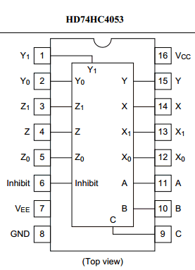
PIN ASSIGNMENT
LOGIC DIAGRAM
Triple Single-Pole, Double-Position
Plus Common Off
PIN 16 =VCC
PIN 7 = VEE
PIN 8 = GND
SLS
System Logic
Semiconductor
FUNCTION TABLE
Control Inputs
Enable
Select
C BA
L LLL
L L LH
L LHL
L L HH
L HLL
L H LH
L HHL
L HHH
H XXX
X = don’t care
ON
Channels
Z0 Y0
Z0 Y0
Z0 Y1
Z0 Y1
Z1 Y0
Z1 Y0
Z1 Y1
Z1 Y1
None
X0
X1
X0
X1
X0
X1
X0
X1
1 page 
SL74HC4053
ADDITIONAL APPLICATION CHARACTERISTICS (GND = 0.0 V)
Symbol
Parameter
Test Conditions
VCC
V
BW Maximum On- fin=1 MHz Sine Wave
Channel
Adjust fin Voltage to Obtain 0 dBm at VOS
Bandwidth or Increase fin Frequence Until dB Meter
Minimum
Reads -3 dB
Frequency
Response
RL =50 Ω, CL=10 pF
(Figure 5)
2.25
4.50
6.00
- Off-Channel fin= Sine Wave
Feedthrough
Adjust fin Voltage to Obtain 0 dBm at VIS
Isolation
fin = 10 kHz, RL =600 Ω, CL=50 pF
(Figure 6)
2.25
4.50
6.00
fin = 1.0 MHz, RL =50 Ω, CL=10 pF
2.25
4.50
6.00
- Feedthrough VIN≤ 1 MHz Square Wave (tr = tf = 6 ns)
Noise, Channel Adjust RL at Setup so that IS= 0 A Enable =
Select Input to GND
Common O/I
RL =600 Ω, CL=50 pF
2.25
(Figure 7)
4.50
6.00
RL =10 Ω, CL=10 pF
2.25
4.50
6.00
- Crosstalk
fin= Sine Wave
Between Any Adjust fin Voltage to Obtain 0 dBm at VIS
Two Switches
fin = 10 kHz, RL =600 Ω, CL=50 pF
(Figure 14)
2.25
4.50
6.00
fin = 1 MHz, RL =50 Ω, CL=10 pF
2.25
4.50
6.00
THD
Total Harmonic
Distortion
(Figure 16)
fin= 1 kHz, RL =10 kΩ, CL=50 pF
THD = THDMeasured - THDSource
VIS =4.0 VPP sine wave
VIS =8.0 VPP sine wave
VIS =11.0 VPP sine wave
* Limits not tested. Determined by design and verified by qualification.
2.25
4.50
6.00
VEE
V
-2.25
-4.50
-6.00
-2.25
-4.50
-6.00
-2.25
-4.50
-6.00
-2.25
-4.50
-6.00
-2.25
-4.50
-6.00
-2.25
-4.50
-6.00
-2.25
-4.50
-6.00
-2.25
-4.50
-6.00
Limit*
25 °C
Unit
MHz
120
120
120
dB
-50
-50
-50
-40
-40
-40
mVpp
25
105
135
35
145
190
dB
-50
-50
-50
-60
-60
-60
%
0.10
0.08
0.05
SLS
System Logic
Semiconductor
5 Page | ||

| Páginas | Total 8 Páginas | |
| PDF Descargar | [ Datasheet HC4053.PDF ] | |
Hoja de datos destacado
| Número de pieza | Descripción | Fabricantes |
| HC4052 | Dual 4-channel analog multiplexer/demultiplexer | NXP Semiconductors |
| HC4052 | Dual 4-channel/ Triple 2-channel Analog Multiplexers/Demultiplexers/ | Hitachi Semiconductor |
| HC4052 | 8-Channel Analog Multiplexer . Dual 4-Channel Analog Multiplexer . Triple 2-Channel Analog Multiplexer | Fairchild Semiconductor |
| HC4052 | ANALOGMULTIPLEXER/DEMULTIPLEXER: SINGLE8CHANNEL/ DUAL 4CHANNEL/ TRIPLE2CHANNEL | STMicroelectronics |
| Número de pieza | Descripción | Fabricantes |
| SLA6805M | High Voltage 3 phase Motor Driver IC. |
Sanken |
| SDC1742 | 12- and 14-Bit Hybrid Synchro / Resolver-to-Digital Converters. |
Analog Devices |
|
DataSheet.es es una pagina web que funciona como un repositorio de manuales o hoja de datos de muchos de los productos más populares, |
| DataSheet.es | 2020 | Privacy Policy | Contacto | Buscar |