|
|
|
PDF HC55185 Data sheet ( Hoja de datos )
| Número de pieza | HC55185 | |
| Descripción | VoIP Ringing SLIC Family | |
| Fabricantes | Intersil Corporation | |
| Logotipo | ||
Hay una vista previa y un enlace de descarga de HC55185 (archivo pdf) en la parte inferior de esta página. Total 17 Páginas | ||
|
No Preview Available !
TM
Data Sheet
HC55185
April 2000 File Number 4831.2
VoIP Ringing SLIC Family
The RSLIC-VoIP family of
ringing subscriber line
interface circuits (RSLIC)
supports analog Plain Old
Telephone Service (POTS) in
short and medium loop length, wireless and wireline
applications. Ideally suited for remote subscriber units, this
family of products offers flexibility to designers with high
ringing voltage and low power consumption system
requirements.
The RSLIC-VoIP family operates to 100V which translates
directly to the amount of ringing voltage supplied to the end
subscriber. With the high operating voltage, subscriber loop
lengths can be extended to 500Ω (i.e., 5,000 feet) and
beyond.
Other key features across the product family include: low
power consumption, ringing using sinusoidal or trapezoidal
waveforms, robust auto-detection mechanisms for when
subscribers go on or off hook, and minimal external discrete
application components. Integrated test access features are
also offered on selected products to support loopback
testing as well as line measurement tests.
There are five product offerings of the HC55185 with each
version providing voltage grades of high battery voltage and
longitudinal balance. The voltage feed amplifier design uses
low fixed loop gains to achieve high analog performance with
low susceptibility to system induced noise.
Features
• Onboard Ringing Generation
• Compatible with Existing HC5518x Devices
• Low Standby Power Consumption (75V, 65mW)
• Reduced Idle Channel Noise
• Programmable Transient Current Limit
• Improved Off Hook Software Interface
• Integrated MTU DC Characteristics
• Low External Component Count
• Silent Polarity Reversal
• Pulse Metering and On Hook Transmission
• Tip Open Ground Start Operation
• Thermal Shutdown with Alarm Indicator
• 28 Lead Surface Mount Packaging
• Dielectric Isolated (DI) High Voltage Design
Applications
• Voice Over Internet Protocol (VoIP)
• Cable Modems
• Voice Over DSL (VoDSL)
• Short Loop Access Platforms
• Remote Subscriber Units
• Terminal Adapters
Related Literature
• AN9814, User’s Guide for Development Board
• AN9824, Modeling of the AC Loop
• Interfacing to DSP CODECs (Contact Factory)
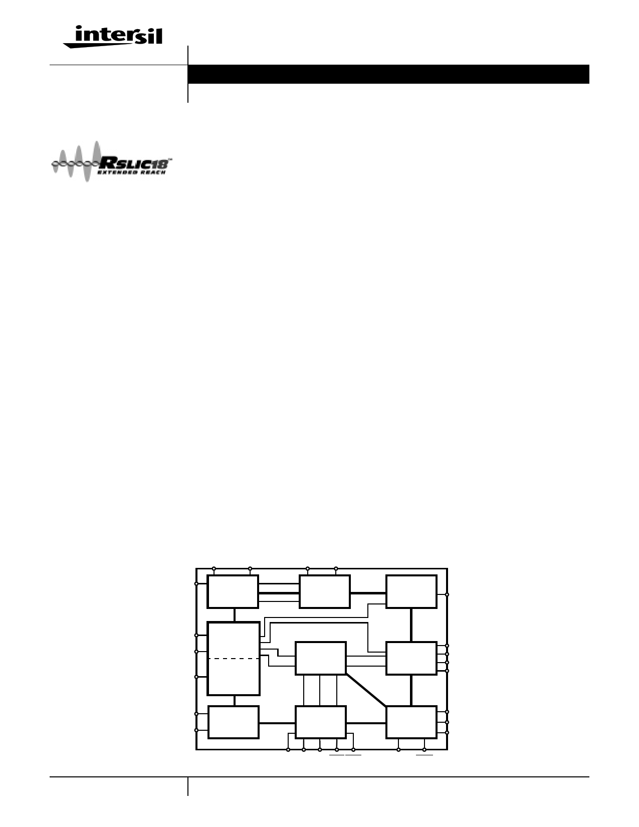
Block Diagram
POL
CDC
VBL VBH
ILIM
DC
CONTROL
BATTERY
SWITCH
RINGING
PORT
VRS
TIP
RING
TL
2-WIRE
PORT
TRANSIENT
CURRENT
LIMIT
TRANSMIT
SENSING
4-WIRE
PORT
VRX
VTX
-IN
VFB
SW+
SW-
TEST
ACCESS
DETECTOR
LOGIC
CONTROL
LOGIC
F2
F1
F0
RTD RD E0 DET ALM
BSEL SWC
4-1
CAUTION: These devices are sensitive to electrostatic discharge; follow proper IC Handling Procedures.
1-888-INTERSIL or 321-724-7143 | Intersil and Design is a trademark of Intersil Corporation. | Copyright © Intersil Corporation 2000
RSLIC18™ is a trademark of Intersil Corporation.
1 page 
HC55185
Electrical Specifications
Unless Otherwise Specified, TA = -40oC to 85oC for industrial (I) grade and TA = 0oC to 85oC for commercial
(C) grade, VBL = -24V, VBH = -100V, -85V or -75V, VCC = +5V, AGND = BGND = 0V, loop current limit = 25mA.
All AC parameters are specified at 600Ω 2-wire terminating impedance over the frequency band of 300Hz to
3.4kHz. Protection resistors = 0Ω.
PARAMETER
TEST CONDITIONS
MIN TYP MAX UNITS
LOGIC INPUTS (F0, F1, F2, E0, SWC)
Input Low Voltage
-
- 0.8
V
Input High Voltage
2.0 -
-
V
Input Low Current
Input High Current
LOGIC OUTPUTS (DET, ALM)
VIL = 0.4V
VIH = 2.4V
-20 - - µA
- - 1 µA
Output Low Voltage
Output High Voltage
SUPPLY CURRENTS
IOL = 5mA
IOH = 100µA
- .15 0.4
2.4 3.5
-
V
V
Low Power Standby, BSEL = 1
Forward or Reverse, BSEL = 0
Forward, BSEL = 1
Ringing, BSEL = 1
Forward Loopback, BSEL = 0
Tip Open, BSEL = 0
Power Denial, BSEL = 0 or 1
ON HOOK POWER DISSIPATION (Note 6)
ICC
IBH
ICC
IBL
ICC
IBL
IBH
ICC
IBL
IBH
ICC
IBL
ICC
IBL
ICC
IBL
-
3.9 6.0
mA
- 0.66 0.90 mA
-
4.9 6.5
mA
-
1.2 2.5
mA
-
7.0 9.5
mA
-
0.9 2.0
mA
-
2.2 3.0
mA
-
6.4 9.0
mA
-
0.3 1.0
mA
-
2.0 3.0
mA
- 10.3 13.5 mA
- 23.5 32
mA
-
3.8 5.5
mA
- .3 1.0 mA
-
4.0 6.0
mA
- 0.22 0.5 mA
Forward or Reverse
Low Power Standby
Ringing
OFF HOOK POWER DISSIPATION (Note 6)
VBL = -24V
VBH = -100V
VBH = -85V
VBH = -75V
VBH = -100V
VBH = -85V
VBH = -75V
- 55 -
- 85 -
- 75 -
- 65 -
- 250 -
- 230 -
- 225 -
mW
mW
mW
mW
mW
mW
mW
Forward or Reverse
POWER SUPPLY REJECTION RATIO
VBL = -24V
- 305 -
mW
4-5
5 Page 
HC55185
When RKNEE is exceeded, the device will transition from
constant current feed to constant voltage, resistive feed. The
line segment IB represents the resistive feed portion of the
load characteristic.
IB = V---R--T--L-R--O---(--OO----CP----)
(EQ. 24)
Voice Transmission
The feedback mechanism for monitoring the AC portion of
the loop current consists of two amplifiers, the sense
amplifier (SA) and the transmit amplifier (TA). The AC
feedback signal is used for impedance synthesis. A detailed
model of the AC feed back loop is provided below.
TIP
RING
R
20 -
+
20
+-
R
R
1:1
TA
VRX
VTX
RS
R 4R
3R
-IN
4R CFB
- 8K
4R +
VFB
VSA
4R 3R
FIGURE 7. AC SIGNAL TRANSMISSION MODEL
The gain of the transmit amplifier, set by RS , determines the
programmed impedance of the device. The capacitor CFB
blocks the DC component of the loop current. The ground
symbols in the model represent AC grounds, not actual DC
potentials.
The sense amp output voltage, VSA, as a function of Tip and
Ring voltage and load is calculated using Equation 25.
VSA = –(VT – VR)-Z3---0L--
(EQ. 25)
The transmit amplifier provides the programmable gain
required for impedance synthesis. In addition, the output of
this amplifier interfaces to the CODEC transmit input. The
output voltage is calculated using Equation 26.
VVTX
=
–VSA
8--R--e---S-3--
(EQ. 26)
Once the impedance matching components have been
selected using the design equations, the above equations
provide additional insight as to the expected AC node
voltages for a specific Tip and Ring load.
Transhybrid Balance
The final step in completing the impedance synthesis design
is calculating the necessary gains for transhybrid balance.
The AC feed back loop produces an echo at the VTX output
of the signal injected at VRX. The echo must be cancelled to
4-11
maintain voice quality. Most applications will use a summing
amplifier in the CODEC front end as shown below to cancel
the echo signal.
R
R
1:1
TA
HC5518x
VRX
VTX
RS
-IN
RA
RB RF
RX OUT
-
+
TX IN
+2.4V
CODEC
FIGURE 8. TRANSHYBRID BALANCE INTERFACE
The resistor ratio, RF/RB, provides the final adjustment for
the transmit gain, GTX. The transmit gain is calculated using
Equation 27.
TX
=
–G24
R-R----BF--
(EQ. 27)
Most applications set RF = RB, hence the device 2-wire to
4-wire equals the transmit gain. Typically RB is greater than
20kΩ to prevent loading of the device transmit output.
The resistor ratio, RF/RA, is determined by the transhybrid
gain of the device, G44. RF is previously defined by the
transmit gain requirement and RA is calculated using
Equation 28.
RA= G--R---4-B--4--
(EQ. 28)
Power Dissipation
The power dissipated by the device during on hook
transmission is strictly a function of the quiescent currents
for each supply voltage during Forward Active operation.
PFAQ=
VBH
×
I
B
H
Q
+
VB
L
×
IB
L
Q
+
VCC
×
ICCQ
(EQ. 29)
Off hook power dissipation is increased above the quiescent
power dissipation by the DC load. If the loop length is less
than or equal to RKNEE, the device is providing constant
current, IA, and the power dissipation is calculated using
Equation 30.
PFA(IA) = PFA(Q) + (VBLxIA) – (RLOOPxI2A)
(EQ. 30)
If the loop length is greater than RKNEE , the device is
operating in the constant voltage, resistive feed region. The
power dissipated in this region is calculated using Equation 31.
PFA(IB)= PFA(Q) + (VBLxIB) – (RLOOPxI2B)
(EQ. 31)
Since the current relationships are different for constant
current versus constant voltage, the region of device
operation is critical to valid power dissipation calculations.
11 Page | ||
| Páginas | Total 17 Páginas | |
| PDF Descargar | [ Datasheet HC55185.PDF ] | |
Hoja de datos destacado
| Número de pieza | Descripción | Fabricantes |
| HC55180 | Extended Reach Ringing SLIC Family | Intersil Corporation |
| HC55181 | Extended Reach Ringing SLIC Family | Intersil Corporation |
| HC55182 | Extended Reach Ringing SLIC Family | Intersil Corporation |
| HC55183 | Extended Reach Ringing SLIC Family | Intersil Corporation |
| Número de pieza | Descripción | Fabricantes |
| SLA6805M | High Voltage 3 phase Motor Driver IC. |
Sanken |
| SDC1742 | 12- and 14-Bit Hybrid Synchro / Resolver-to-Digital Converters. |
Analog Devices |
|
DataSheet.es es una pagina web que funciona como un repositorio de manuales o hoja de datos de muchos de los productos más populares, |
| DataSheet.es | 2020 | Privacy Policy | Contacto | Buscar |